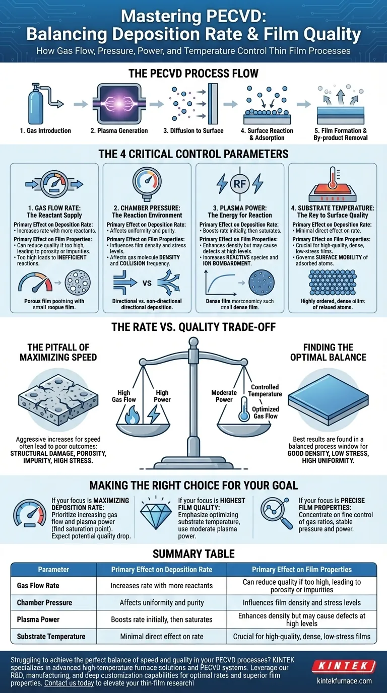
In Plasma-Enhanced Chemical Vapor Deposition (PECVD), deposition rates and film properties are fundamentally controlled by adjusting four key process parameters: gas flow rate, chamber pressure, plasma power, and substrate temperature. These variables are not independent but work together as a system to govern the supply of reactants, the energy of the chemical reactions, and the behavior of atoms on the substrate surface, ultimately defining the final film's thickness, density, and quality.
To master PECVD, one must move beyond simply adjusting individual settings. The core challenge is to understand how these parameters interact to balance two often-competing goals: the speed of deposition and the quality of the resulting film.
The PECVD Process: A Quick Primer
To understand how to control the outcome, it's essential to visualize the process. PECVD is a sequence of steps, and each control parameter influences one or more of these stages.
The Five Key Stages
- Gas Introduction: Precursor gases are fed into the vacuum chamber at a controlled rate.
- Plasma Generation: A high-frequency electric field is applied, stripping electrons from gas molecules and creating an energized plasma filled with ions and reactive free radicals.
- Diffusion to Surface: These highly reactive species move from the plasma toward the substrate.
- Surface Reaction & Adsorption: The species react on the substrate surface, adsorbing and forming the desired material.
- Film Formation & By-product Removal: A solid thin film grows on the substrate, while volatile by-products are desorbed and pumped out of the chamber.
The Four Critical Control Parameters
Each parameter acts as a lever to influence the process, and understanding their specific roles is key to achieving your desired film characteristics.
Gas Flow Rate: The Reactant Supply
The flow rate of your precursor gases directly controls the concentration of reactants available in the chamber.
Increasing the gas flow generally increases the deposition rate because more raw material is supplied for the reaction. However, this effect is not infinite; the rate will eventually be limited by other factors like plasma power or temperature.
Chamber Pressure: The Reaction Environment
Pressure influences the density of gas molecules and their mean free path—the average distance a particle travels before colliding with another.
Lower pressure leads to fewer gas-phase collisions and more directional deposition, while higher pressure increases collisions, which can sometimes create unwanted particles. Pressure critically affects the uniformity and purity of the film.
Plasma Power: The Energy for Reaction
The radio-frequency (RF) power applied to the chamber dictates the energy of the plasma. Higher power creates a denser plasma with more free radicals.
Initially, increasing power boosts the deposition rate by generating more reactive species. It also increases ion bombardment on the substrate, which can improve film density. However, after a certain point, the precursor gas becomes fully ionized, the radical concentration saturates, and the deposition rate stabilizes.
Substrate Temperature: The Key to Surface Quality
Temperature governs the energy of the substrate surface itself. It does not create the reactants (like plasma does), but it dictates what happens to them once they arrive.
Higher temperatures give adsorbed atoms more surface mobility, allowing them to settle into more ordered, stable positions. This is crucial for forming denser, less stressed, and higher-quality films. PECVD's main advantage is its ability to achieve this at relatively low temperatures (under 400°C).
Understanding the Trade-offs: Rate vs. Quality
It is a common mistake to tune parameters with only one goal in mind. The most frequent trade-off in PECVD is between the deposition rate and the final film quality.
The Pitfall of Maximizing Speed
Pushing for the fastest possible deposition rate by aggressively increasing gas flow and plasma power often leads to poor outcomes.
High power can cause excessive ion bombardment, leading to structural damage or defects in the film. Similarly, a very high gas flow can result in inefficient reactions, producing a film that is porous, impure, or has high internal stress.
Finding the Optimal Balance
The best results are typically found in a balanced process window. For example, a moderately high power level might be used to ensure good density, while a controlled temperature ensures atoms can arrange properly to relieve stress. The gas flow is then set to supply reactants without overwhelming the system.
Making the Right Choice for Your Goal
Your optimal process recipe depends entirely on what you prioritize. Use these guidelines as a starting point for developing your own process.
- If your primary focus is maximizing deposition rate: Prioritize increasing the gas flow rate and plasma power, but be prepared for a potential drop in film quality and find the saturation point where more power yields no benefit.
- If your primary focus is the highest film quality (density, low stress): Emphasize optimizing the substrate temperature to enhance surface mobility and use a moderate plasma power to avoid damage.
- If your primary focus is precise film properties (refractive index, stoichiometry): Concentrate on achieving fine control over the ratios of different precursor gases and maintaining exceptionally stable pressure and power throughout the deposition.
Ultimately, mastering PECVD is about methodically tuning this interconnected system to achieve the precise balance of film properties your application demands.
Summary Table:
| Parameter | Primary Effect on Deposition Rate | Primary Effect on Film Properties |
|---|---|---|
| Gas Flow Rate | Increases rate with more reactants | Can reduce quality if too high, leading to porosity or impurities |
| Chamber Pressure | Affects uniformity and purity | Influences film density and stress levels |
| Plasma Power | Boosts rate initially, then saturates | Enhances density but may cause defects at high levels |
| Substrate Temperature | Minimal direct effect on rate | Crucial for high-quality, dense, low-stress films |
Struggling to achieve the perfect balance of speed and quality in your PECVD processes? KINTEK specializes in advanced high-temperature furnace solutions, including our precision-engineered PECVD systems. Leveraging exceptional R&D and in-house manufacturing, we provide diverse laboratories with tailored solutions that ensure optimal deposition rates and superior film properties. Our strong deep customization capability allows us to precisely meet your unique experimental needs, whether you're focused on maximizing throughput or enhancing film density. Contact us today to discuss how KINTEK can elevate your thin-film research and production!
Visual Guide
Related Products
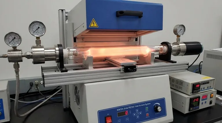
- RF PECVD System Radio Frequency Plasma Enhanced Chemical Vapor Deposition
- Slide PECVD Tube Furnace with Liquid Gasifier PECVD Machine
- Inclined Rotary Plasma Enhanced Chemical Deposition PECVD Tube Furnace Machine
- Inclined Rotary Plasma Enhanced Chemical Deposition PECVD Tube Furnace Machine
- Cylindrical Resonator MPCVD Machine System for Lab Diamond Growth
People Also Ask
- What are the applications of plasma enhanced chemical vapor deposition? Key Uses in Electronics, Optics & Materials
- How does film quality compare between PECVD and CVD? Choose the Best Method for Your Substrate
- How is silicon dioxide deposited from tetraethylorthosilicate (TEOS) in PECVD? Achieve Low-Temperature, High-Quality SiO2 Films
- What are some promising applications of PECVD-prepared 2D materials? Unlock Advanced Sensing and Optoelectronics
- What is RF in PECVD? A Critical Control for Plasma Deposition


