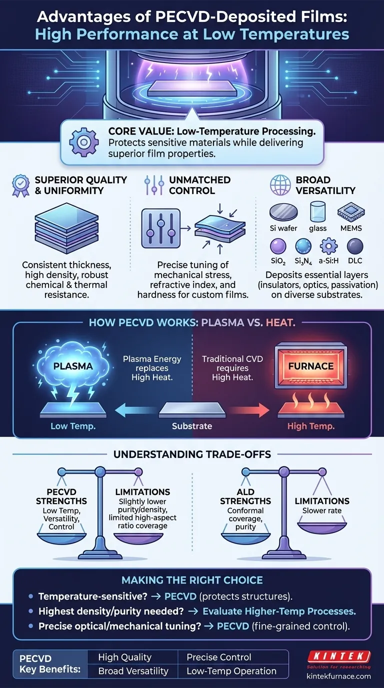
From a technical standpoint, Plasma-Enhanced Chemical Vapor Deposition (PECVD) films are prized for their exceptional uniformity, high quality, and robust resistance to chemical and thermal stress. The primary advantage of the PECVD process is its ability to produce these high-performance films at significantly lower temperatures than conventional CVD, enabling precise control over material properties like stress, refractive index, and hardness.
The core value of PECVD is not just the quality of the films it produces, but its ability to do so at low temperatures. By using plasma to drive chemical reactions instead of high heat, PECVD unlocks the ability to deposit critical insulating, optical, and protective layers on a vast range of materials without causing thermal damage.
The Core Advantages of PECVD Films
PECVD has become a cornerstone technology in fabricating semiconductors, optics, and MEMS devices. The advantages stem directly from the plasma-driven nature of the process.
Superior Film Quality and Uniformity
PECVD films are known for their consistent thickness and structural integrity across the entire substrate. They are highly cross-linked, which makes them dense and resistant to cracking.
This robust structure also provides excellent resistance to chemical attack and thermal changes, making them ideal for protective layers.
Unmatched Control Over Material Properties
The process allows for fine-tuning of critical film characteristics. Engineers can precisely manipulate the resulting film's mechanical stress, which is vital for preventing delamination or cracking in complex device structures.
Furthermore, properties like the refractive index and hardness can be adjusted by changing process parameters, enabling the creation of custom optical coatings and durable hard masks.
Broad Material and Application Versatility
PECVD is not limited to a single material. It is used to deposit a wide array of essential films, including silicon oxide (SiO2), silicon nitride (Si3N4), amorphous silicon (a-Si:H), and even diamond-like carbon (DLC).
This versatility makes it indispensable for countless applications, from electrical insulators and passivation layers in microchips to anti-reflective coatings on lenses and sacrificial layers in MEMS devices.
How PECVD Achieves These Results
The unique benefits of PECVD are a direct result of using plasma to energize the deposition process. Understanding this mechanism is key to leveraging the technology effectively.
Overcoming Thermal Limitations
In traditional Chemical Vapor Deposition (CVD), very high temperatures are required to provide enough energy to break down precursor gases and initiate a chemical reaction on the substrate surface.
PECVD replaces this reliance on high heat with energy from a plasma. The plasma creates highly reactive ions and radicals from the precursor gases at a much lower temperature, allowing deposition to occur on substrates that could not withstand a high-thermal process.
Enhanced Reactivity and Deposition Control
The reactive species created in the plasma increase the efficiency of the deposition reactions. This allows for better control over the film's final composition and microstructure.
By manipulating the plasma environment, engineers can influence how the film grows, achieving desirable traits like conformal step coverage over complex topographies or dense, void-free films.
The Importance of Process Parameters
The precise control offered by PECVD comes from the ability to adjust several key process "levers." These include:
- Gas flow rates: Determines the chemical composition of the film.
- Plasma power: Influences reactant density and ion energy.
- Chamber pressure: Affects the mean free path of particles and deposition uniformity.
- Substrate temperature: Modifies surface mobility and film stress.
By carefully managing these parameters, a specific, repeatable film with desired properties can be reliably produced.
Understanding the Trade-offs
While powerful, PECVD is not a universal solution. An objective assessment requires acknowledging its limitations.
Film Purity and Density
The lower deposition temperature and plasma environment can sometimes lead to the incorporation of other elements, such as hydrogen, into the film.
Additionally, PECVD films can occasionally be less dense and have slightly lower dielectric strength compared to films deposited at very high temperatures using methods like Low-Pressure CVD (LPCVD).
Conformal Coverage Limitations
While PECVD offers good conformal coverage for many applications, it may not be sufficient for the most demanding, high-aspect-ratio structures found in advanced semiconductors.
In these extreme cases, processes like Atomic Layer Deposition (ALD) often provide superior, more truly conformal coatings, albeit typically at a slower deposition rate.
Making the Right Choice for Your Application
Selecting the right deposition method depends entirely on your project's specific constraints and performance targets.
- If your primary focus is processing temperature-sensitive materials: PECVD is often the superior choice due to its low-temperature operation, which protects underlying device structures.
- If your primary focus is achieving the highest possible film density and purity: You may need to evaluate higher-temperature processes, weighing the benefits against your thermal budget constraints.
- If your primary focus is precise tuning of optical or mechanical properties: The fine-grained control offered by PECVD's process parameters makes it an ideal candidate for creating custom films.
Ultimately, PECVD is a powerful and versatile tool when its unique capabilities are correctly matched to the engineering goal.
Summary Table:
| Advantage | Key Benefit |
|---|---|
| Superior Film Quality | High uniformity, density, and resistance to chemical/thermal stress |
| Unmatched Control | Precise tuning of stress, refractive index, and hardness |
| Broad Versatility | Deposits materials like SiO2, Si3N4 for various applications |
| Low-Temperature Operation | Enables use on temperature-sensitive substrates without damage |
Unlock the full potential of your laboratory with KINTEK's advanced PECVD solutions! Leveraging exceptional R&D and in-house manufacturing, we provide diverse labs with high-performance furnace systems, including CVD/PECVD Systems, tailored to your unique needs. Our strong deep customization capability ensures precise alignment with your experimental requirements, enhancing efficiency and innovation. Contact us today to discuss how we can elevate your research and development processes!
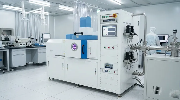
Visual Guide
Related Products
- RF PECVD System Radio Frequency Plasma Enhanced Chemical Vapor Deposition
- Slide PECVD Tube Furnace with Liquid Gasifier PECVD Machine
- Inclined Rotary Plasma Enhanced Chemical Deposition PECVD Tube Furnace Machine
- Inclined Rotary Plasma Enhanced Chemical Deposition PECVD Tube Furnace Machine
People Also Ask
- What are some promising applications of PECVD-prepared 2D materials? Unlock Advanced Sensing and Optoelectronics
- What is PECVD specification? A Guide to Choosing the Right System for Your Lab
- How are deposition rates and film properties controlled in PECVD? Master Key Parameters for Optimal Thin Films
- What is RF in PECVD? A Critical Control for Plasma Deposition
- What is the role of RF power in PECVD and how does the RF-PECVD process work? Master Thin Film Deposition Control


