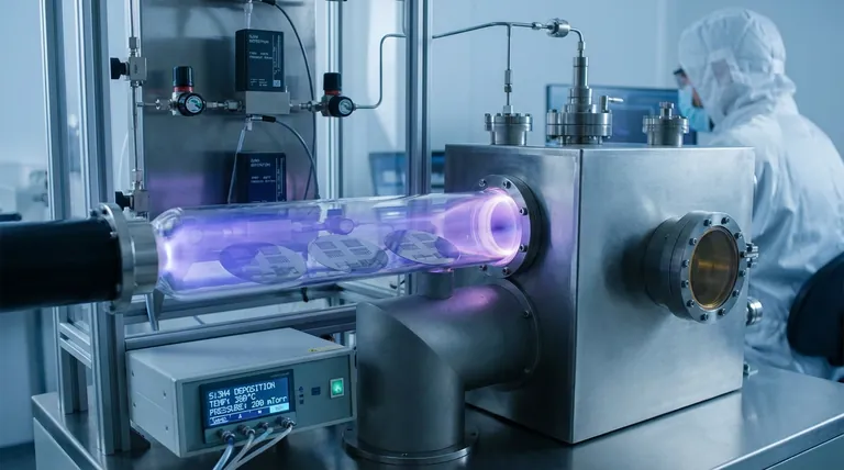
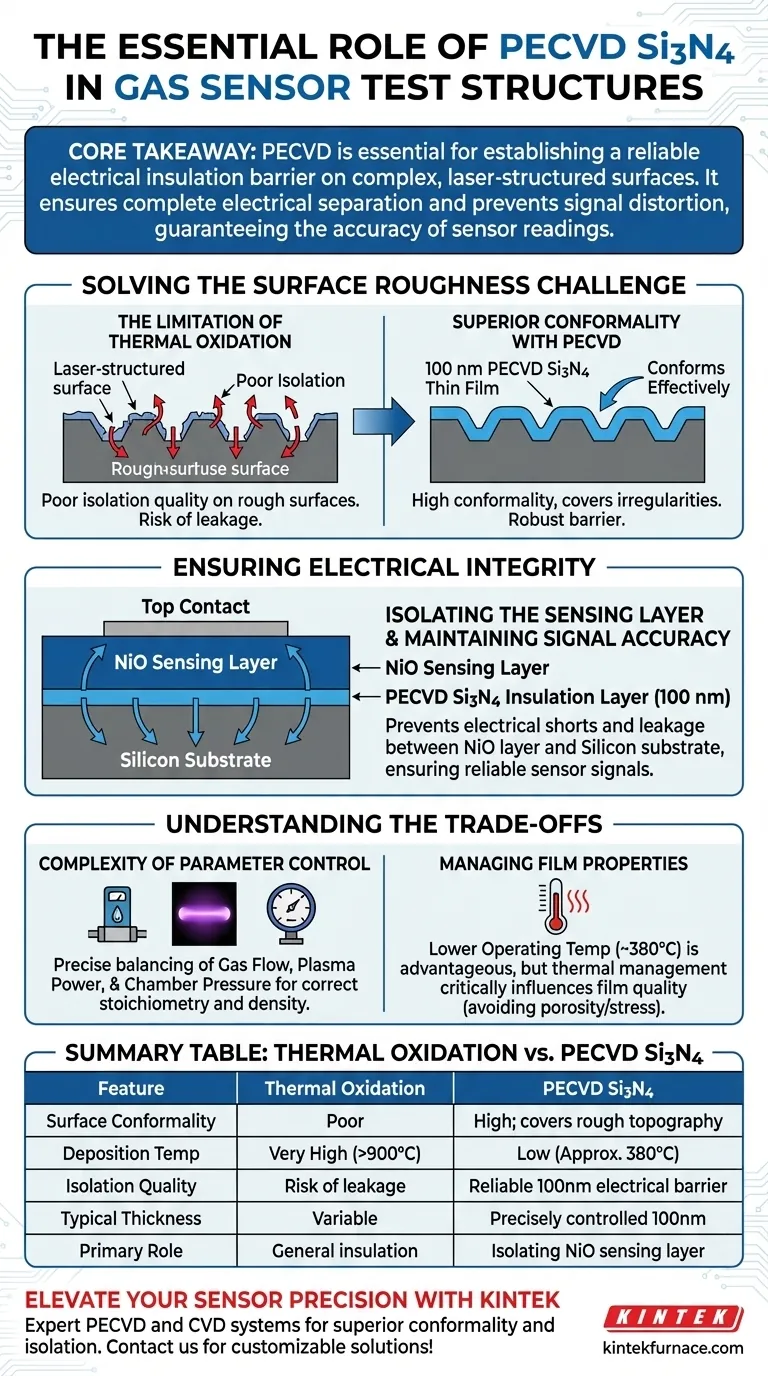
The primary function of Plasma Enhanced Chemical Vapor Deposition (PECVD) in gas sensor test structures is to establish a reliable electrical insulation barrier on complex, laser-structured surfaces. By depositing an approximately 100 nm thick silicon nitride (Si3N4) film, this process effectively isolates the sensor's active layers to prevent signal distortion.
Core Takeaway: PECVD is essential because it overcomes the poor isolation quality associated with thermal oxidation on rough, laser-structured surfaces. It ensures complete electrical separation between the nickel oxide sensing layer and the silicon substrate, guaranteeing the accuracy of sensor readings.
Solving the Surface Roughness Challenge
The decision to use PECVD is driven by the physical topography of the sensor device, specifically the challenges introduced by laser structuring.
The Limitation of Thermal Oxidation
In standard semiconductor manufacturing, thermal oxidation is often used to create insulation layers. However, on rough, laser-structured surfaces, this method frequently results in poor isolation quality.
Superior Conformality
PECVD solves this by growing a 100 nm thick silicon nitride (Si3N4) thin film that conforms effectively to the structured surface. This film acts as a robust barrier, filling the gaps and covering irregularities that traditional oxidation methods might miss.
Ensuring Electrical Integrity
Beyond addressing surface roughness, the Si3N4 layer plays a specific functional role in the sensor's electronic architecture.
Isolating the Sensing Layer
The gas sensor structure typically consists of an upper nickel oxide (NiO) sensing layer and an underlying conductive silicon substrate. These two components must remain electrically distinct for the device to function.
Maintaining Signal Accuracy
The PECVD-deposited Si3N4 film prevents electrical shorts and leakage currents between the NiO layer and the silicon substrate. This isolation is non-negotiable for maintaining the accuracy and reliability of the sensor signals during operation.
Understanding the Trade-offs
While PECVD offers superior isolation for this application, it introduces specific process variables that must be carefully managed to avoid defects.
Complexity of Parameter Control
Unlike simpler thermal processes, PECVD requires the precise balancing of multiple variables. Gas flow rates, plasma power, and chamber pressure must be tightly controlled to achieve the correct film stoichiometry and density.
Managing Film Properties
Although PECVD is advantageous for its lower operating temperatures (often around 380°C), the substrate temperature still critically influences film quality. Improper thermal management can lead to films that are either too porous (poor insulation) or too stressed (prone to cracking).
Making the Right Choice for Your Goal
To ensure your gas sensor functions correctly, apply the following guidelines:
- If your primary focus is signal fidelity: Use PECVD to deposit Si3N4, as it provides the necessary isolation on rough surfaces to prevent electrical interference between the NiO layer and the substrate.
- If your primary focus is thermal budget: leverage PECVD to deposit high-quality insulation films without exposing the substrate to the high temperatures required by traditional furnace processes.
By utilizing PECVD for silicon nitride deposition, you ensure the structural integrity and operational precision of your gas sensor test structures.
Summary Table:
| Feature | Thermal Oxidation | PECVD Si3N4 |
|---|---|---|
| Surface Conformality | Poor on laser-structured surfaces | High; covers rough topography |
| Deposition Temp | Very High (>900°C) | Low (Approx. 380°C) |
| Isolation Quality | Risk of leakage on rough areas | Reliable 100nm electrical barrier |
| Typical Thickness | Variable | Precisely controlled 100nm |
| Primary Role | General substrate insulation | Isolating NiO sensing layer |
Elevate Your Sensor Precision with KINTEK
Don't let signal distortion compromise your research. KINTEK provides industry-leading PECVD and CVD systems designed to deliver superior conformality and electrical isolation for complex gas sensor architectures.
Backed by expert R&D and manufacturing, we offer customizable Muffle, Tube, Rotary, Vacuum, and CVD systems tailored to your unique laboratory needs. Whether you are depositing Si3N4 for insulation or optimizing your thermal budget, our high-temperature solutions ensure the structural integrity and operational precision of your devices.
Ready to optimize your thin-film deposition process? Contact KINTEK today to consult with our technical experts!
Visual Guide
References
- I. Hotový, Fadi Dohnal. Preparation of laser induced periodic surface structures for gas sensing thin films and gas sensing verification of a NiO based sensor structure. DOI: 10.2478/jee-2024-0004
This article is also based on technical information from Kintek Furnace Knowledge Base .
Related Products
- RF PECVD System Radio Frequency Plasma Enhanced Chemical Vapor Deposition
- Inclined Rotary Plasma Enhanced Chemical Deposition PECVD Tube Furnace Machine
- Slide PECVD Tube Furnace with Liquid Gasifier PECVD Machine
- Inclined Rotary Plasma Enhanced Chemical Deposition PECVD Tube Furnace Machine
- Cylindrical Resonator MPCVD Machine System for Lab Diamond Growth
People Also Ask
- What are the advantages of PECVD in film deposition? Achieve Low-Temp, High-Quality Coatings
- What are the system specifications of the PECVD system? Unlock Precision Thin-Film Deposition
- What is the role of RF power in PECVD and how does the RF-PECVD process work? Master Thin Film Deposition Control
- What are some promising applications of PECVD-prepared 2D materials? Unlock Advanced Sensing and Optoelectronics
- What are the limitations of PECVD? Overcome Process Control and Cost Challenges


