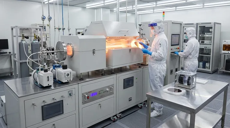
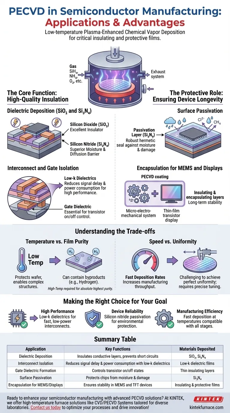
In semiconductor manufacturing, Plasma-Enhanced Chemical Vapor Deposition (PECVD) is the workhorse technology for depositing the critical insulating and protective films that make modern electronics possible. It is used to create layers of silicon dioxide (SiO₂) and silicon nitride (Si₃N₄), which serve as dielectrics to isolate conductive layers, form parts of transistors, and provide a final protective seal for the integrated circuit.
The essential value of PECVD is not just what it deposits, but how it does so: at low temperatures. This single capability is what unlocks the ability to build complex, multi-layered chips without damaging the fragile, temperature-sensitive structures already fabricated on the wafer.
The Core Function: High-Quality Insulation
At its heart, a semiconductor chip is a dense network of switches and wires that must be perfectly insulated from one another. PECVD is the primary tool for building these insulating layers with precision and efficiency.
Dielectric Deposition (SiO₂ and Si₃N₄)
PECVD excels at depositing high-quality dielectric films. These are materials that do not conduct electricity and are fundamental to chip operation.
Silicon dioxide (SiO₂) is an excellent insulator, used to separate different conductive components. Silicon nitride (Si₃N₄) offers superior resistance to moisture and diffusion, making it an ideal protective barrier.
Interconnect and Gate Isolation
Modern chips contain billions of transistors connected by intricate metal "wiring" called interconnects. PECVD deposits insulating layers between these metal lines to prevent short circuits.
For advanced chips, specialized low-k dielectric films are deposited via PECVD. These materials lower the capacitance between wires, reducing signal delay and power consumption, which is critical for high-performance computing.
Forming Transistor Components
PECVD is also used to deposit the gate dielectric, a microscopically thin insulating layer that is essential for controlling the on/off state of a transistor. The quality and integrity of this layer directly impact device performance and reliability.
The Protective Role: Ensuring Device Longevity
Beyond building the active parts of a circuit, PECVD is used to protect the finished product from the outside world.
Surface Passivation
After all the transistors and wiring are in place, the entire chip surface is coated with a final protective layer, a process known as passivation.
A thick layer of silicon nitride deposited by PECVD acts as a robust hermetic seal. This shields the sensitive circuitry from moisture, chemicals, and physical damage that could cause it to fail.
Encapsulation for MEMS and Displays
The same principle applies to other semiconductor devices. In Micro-Electro-Mechanical Systems (MEMS) and the Thin-Film Transistors (TFTs) used in modern displays, PECVD provides the essential insulating and encapsulating layers that ensure long-term stability and function.
Understanding the Trade-offs
No technology is without its compromises. The primary advantage of PECVD—its low operating temperature—defines its relationship with other deposition methods.
Temperature vs. Film Purity
The plasma in a PECVD process provides the energy for chemical reactions, replacing the high heat used in traditional Chemical Vapor Deposition (CVD). While this protects the wafer, the resulting films can sometimes contain byproducts like hydrogen.
For most applications, this is perfectly acceptable. However, for a few select layers that demand the absolute highest purity, a high-temperature process might be chosen if the device structure can withstand it.
Speed vs. Uniformity
PECVD is valued for its relatively fast deposition rates, which increases manufacturing throughput. However, achieving a perfectly uniform film thickness across the entire wafer can be a challenge.
Process engineers must carefully tune gas flows, pressure, and plasma power to balance the need for speed with the strict uniformity requirements of modern semiconductor fabrication.
Making the Right Choice for Your Goal
PECVD is not just one application, but a versatile platform used to achieve different outcomes throughout the fabrication process.
- If your primary focus is high performance: PECVD is non-negotiable for depositing the low-k dielectric materials needed to enable fast, low-power interconnects in advanced logic chips.
- If your primary focus is device reliability: PECVD is the industry standard for creating the final silicon nitride passivation layer that protects the chip from environmental hazards.
- If your primary focus is manufacturing efficiency: PECVD provides a powerful combination of fast deposition rates and high-quality films at temperatures compatible with nearly every stage of device manufacturing.
Ultimately, PECVD's unique ability to create high-quality films at low temperatures makes it an indispensable tool for building the dense and complex integrated circuits that power our world.
Summary Table:
| Application | Key Functions | Materials Deposited |
|---|---|---|
| Dielectric Deposition | Insulates conductive layers, prevents short circuits | SiO₂, Si₃N₄ |
| Interconnect Isolation | Reduces signal delay and power consumption with low-k dielectrics | Low-k dielectric films |
| Gate Dielectric Formation | Controls transistor on/off states | Thin insulating layers |
| Surface Passivation | Protects chips from moisture and damage | Si₃N₄ |
| Encapsulation for MEMS/Displays | Ensures stability in MEMS and TFT devices | Insulating and protective films |
Ready to enhance your semiconductor manufacturing with advanced PECVD solutions? At KINTEK, we leverage exceptional R&D and in-house manufacturing to provide high-temperature furnace solutions like CVD/PECVD Systems, tailored for diverse laboratories. Our strong deep customization capability ensures we precisely meet your unique experimental needs for insulation, protection, and efficiency. Contact us today to discuss how our products can optimize your processes and drive innovation!
Visual Guide
Related Products
- Slide PECVD Tube Furnace with Liquid Gasifier PECVD Machine
- RF PECVD System Radio Frequency Plasma Enhanced Chemical Vapor Deposition
- Inclined Rotary Plasma Enhanced Chemical Deposition PECVD Tube Furnace Machine
- Inclined Rotary Plasma Enhanced Chemical Deposition PECVD Tube Furnace Machine
- Multi Heating Zones CVD Tube Furnace Machine for Chemical Vapor Deposition Equipment
People Also Ask
- What are the typical conditions for plasma-enhanced CVD processes? Achieve Low-Temperature Thin Film Deposition
- How does PECVD equipment contribute to TOPCon bottom cells? Mastering Hydrogenation for Maximum Solar Efficiency
- In which industries is the tube furnace commonly used? Essential for Materials Science, Energy, and More
- What are the disadvantages of tube furnace cracking when processing heavy raw materials? Avoid Costly Downtime and Inefficiency
- What are the advantages of using a tube furnace CVD system for Cu(111)/graphene? Superior Scalability and Quality


