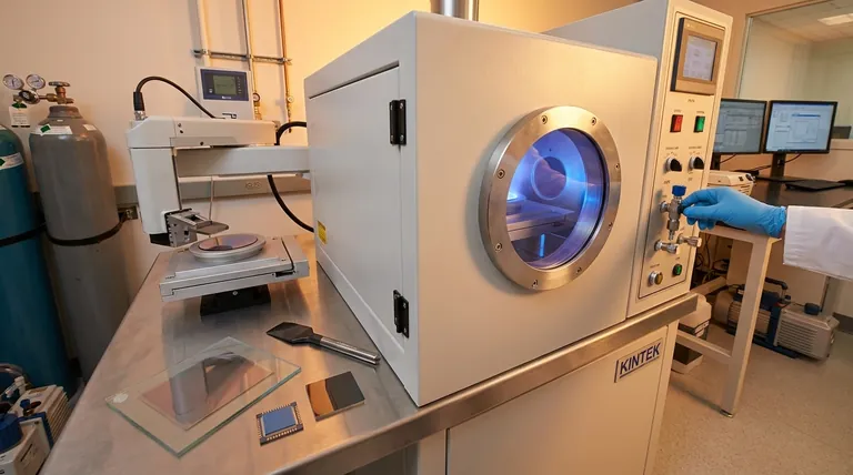
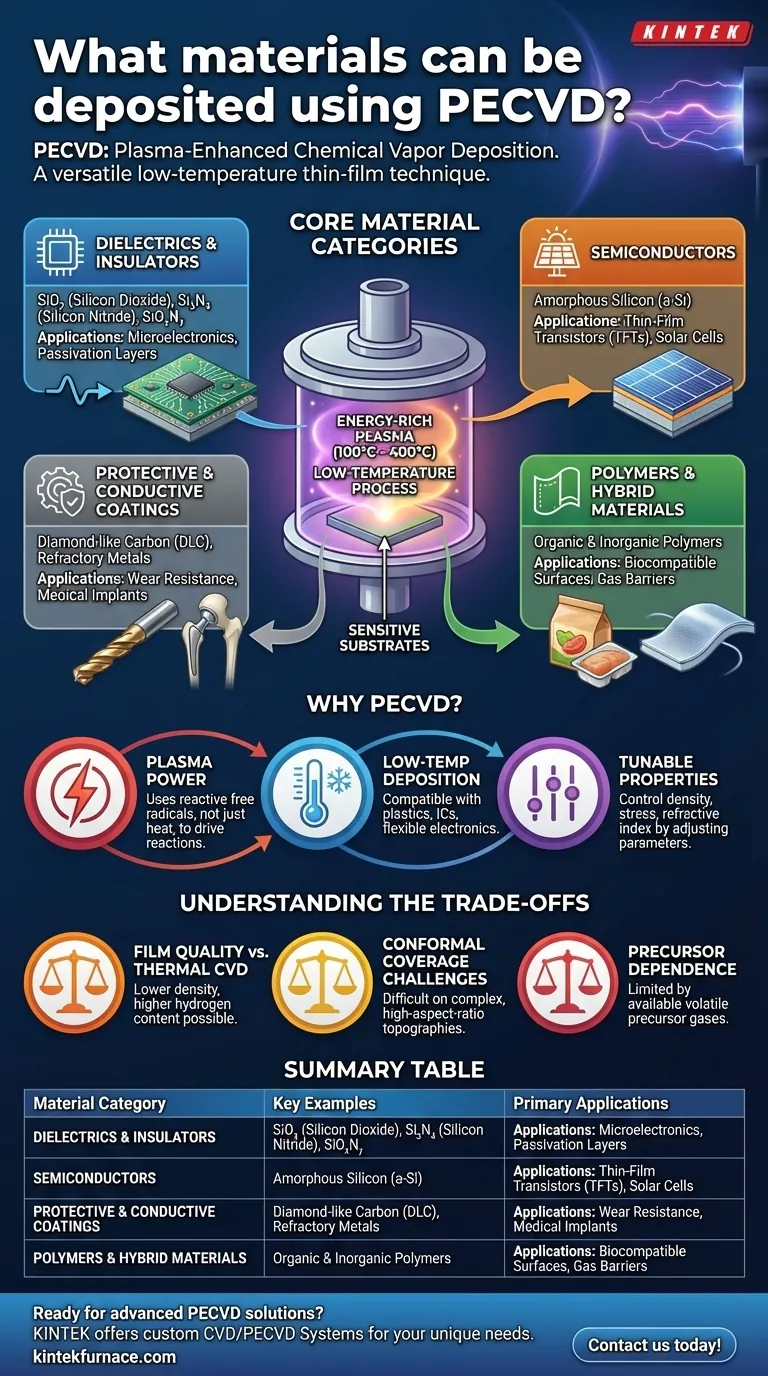
At its core, Plasma-Enhanced Chemical Vapor Deposition (PECVD) is a highly versatile thin-film deposition technique capable of depositing a vast range of materials. These materials fall into several key categories, including dielectric insulators like silicon dioxide (SiO₂) and silicon nitride (Si₃N₄), semiconductors such as amorphous silicon (a-Si), and protective coatings like diamond-like carbon (DLC). The process can also be used for metals, various polymers, and complex hybrid structures.
The true power of PECVD lies not just in the variety of materials it can deposit, but in its ability to do so at low temperatures. This is because it uses an energy-rich plasma, rather than high heat, to drive the necessary chemical reactions, making it compatible with sensitive substrates that other methods would destroy.
The Core Material Categories of PECVD
PECVD's versatility stems from its ability to tailor process chemistry to produce films with specific electrical, mechanical, or optical properties. The materials deposited are fundamental to countless modern technologies.
Dielectrics and Insulators
This is the most common application for PECVD, especially in microelectronics. These films are used to electrically isolate conductive layers from one another.
The primary materials are silicon dioxide (SiO₂) and silicon nitride (Si₃N₄). SiO₂ serves as an excellent insulator, while Si₃N₄ is a superior barrier against moisture and ionic contamination, making it an ideal passivation layer to protect the final device. Silicon oxynitride (SiOxNy) combines properties of both.
Semiconductors
PECVD is crucial for depositing semiconductor films, particularly on large areas or on substrates that cannot withstand high temperatures.
The most notable material is amorphous silicon (a-Si), which is essential for thin-film transistors (TFTs) used in LCD displays and for large-area solar cells. The process also allows for in-situ doping, where dopant gases are added during deposition to create n-type or p-type semiconductor layers directly.
Protective and Conductive Coatings
Beyond electronics, PECVD is used to create films that enhance the physical properties of a surface.
Diamond-like Carbon (DLC) is a key example. It creates an extremely hard, low-friction, and wear-resistant surface, used on everything from machine tools to medical implants. PECVD can also deposit certain refractory metals and their silicides, which serve as conductive layers or diffusion barriers in integrated circuits.
Polymers and Hybrid Materials
The low-temperature nature of PECVD allows for the deposition of organic and inorganic polymer films. These have specialized uses, such as creating biocompatible surfaces on medical implants or forming high-performance gas barriers for food packaging.
Why PECVD Offers Such Broad Capability
The "what" is impressive, but the "why" is what makes PECVD a cornerstone of materials science. The process mechanics are fundamentally different from traditional thermal methods.
The Role of Plasma, Not Just Heat
In conventional Chemical Vapor Deposition (CVD), high temperatures (often >600°C) are required to break down precursor gases and initiate the chemical reaction. PECVD generates a plasma, an ionized gas containing highly reactive free radicals.
These energetic radicals can drive the deposition reaction at much lower temperatures, typically between 100°C and 400°C.
Low-Temperature Deposition is Key
This low-temperature window is PECVD's defining advantage. It allows for deposition onto materials that would melt, warp, or be otherwise damaged by high-temperature processes.
This includes plastics, fully fabricated integrated circuits with low-melting-point metals like aluminum, and flexible substrates for next-generation electronics.
Tunable Film Properties
The film's final characteristics are not fixed. By precisely controlling process parameters—such as gas composition, flow rates, pressure, and RF power—engineers can tune the properties of the deposited film.
This allows for fine-tuning of a material's density, internal stress, refractive index, and electrical resistivity to meet the exact requirements of the application.
Understanding the Trade-offs
No technique is without its compromises. Acknowledging the limitations of PECVD is critical for making an informed decision.
Film Quality vs. Thermal CVD
Because they are deposited at lower temperatures, PECVD films can sometimes have a lower density and higher hydrogen content compared to films grown with high-temperature thermal CVD. This hydrogen comes from the precursor gases (like silane, SiH₄) and can impact the film's electrical stability over time.
Conformal Coverage Challenges
While PECVD provides good coverage, achieving perfectly uniform thickness over complex, high-aspect-ratio topographies (like deep trenches) can be more challenging than with some other deposition methods, such as Atomic Layer Deposition (ALD).
Dependence on Precursor Chemistry
The process is entirely dependent on the availability of suitable precursor gases that are volatile and can be effectively dissociated by the plasma. This can sometimes limit the deposition of more exotic materials.
Making the Right Choice for Your Application
Selecting PECVD depends entirely on your project's goals, constraints, and material requirements.
- If your primary focus is microelectronic insulation: PECVD is the industry standard for depositing high-quality silicon dioxide and silicon nitride passivation layers at temperatures that won't damage the underlying circuitry.
- If your primary focus is mechanical wear resistance: PECVD is the ideal method for applying hard, low-friction Diamond-like Carbon (DLC) coatings to tools, components, and medical devices.
- If your primary focus is flexible electronics or photovoltaics: PECVD is essential for depositing amorphous silicon and other materials onto large-area glass or temperature-sensitive plastic substrates.
- If your primary focus is ultimate film purity and conformality: You may need to compare PECVD with higher-temperature CVD or slower ALD processes, weighing the trade-offs between thermal budget, speed, and film quality.
Ultimately, PECVD's ability to deposit a wide array of functional materials at low temperatures makes it an indispensable and versatile tool in modern engineering and manufacturing.
Summary Table:
| Material Category | Key Examples | Primary Applications |
|---|---|---|
| Dielectrics and Insulators | SiO₂, Si₃N₄, SiOxNy | Microelectronics, passivation layers |
| Semiconductors | Amorphous silicon (a-Si) | Thin-film transistors, solar cells |
| Protective and Conductive Coatings | Diamond-like carbon (DLC), metals | Wear resistance, medical implants |
| Polymers and Hybrid Materials | Organic polymers | Biocompatible surfaces, gas barriers |
Ready to enhance your laboratory with advanced PECVD solutions? At KINTEK, we leverage exceptional R&D and in-house manufacturing to provide diverse labs with high-temperature furnace solutions, including CVD/PECVD Systems. Our strong deep customization capability ensures we can precisely meet your unique experimental requirements. Contact us today to discuss how our tailored PECVD systems can drive your innovations forward!
Visual Guide
Related Products
- Slide PECVD Tube Furnace with Liquid Gasifier PECVD Machine
- RF PECVD System Radio Frequency Plasma Enhanced Chemical Vapor Deposition
- Inclined Rotary Plasma Enhanced Chemical Deposition PECVD Tube Furnace Machine
- Inclined Rotary Plasma Enhanced Chemical Deposition PECVD Tube Furnace Machine
- Multi Heating Zones CVD Tube Furnace Machine for Chemical Vapor Deposition Equipment
People Also Ask
- How does a hydrogen reduction environment in an industrial tube furnace facilitate gold-copper alloy microspheres?
- What are the typical conditions for plasma-enhanced CVD processes? Achieve Low-Temperature Thin Film Deposition
- What plasma source is used in PE-CVD tube furnaces? Unlock Low-Temperature, High-Quality Deposition
- What are the advantages of using a tube furnace CVD system for Cu(111)/graphene? Superior Scalability and Quality
- What are the disadvantages of tube furnace cracking when processing heavy raw materials? Avoid Costly Downtime and Inefficiency


