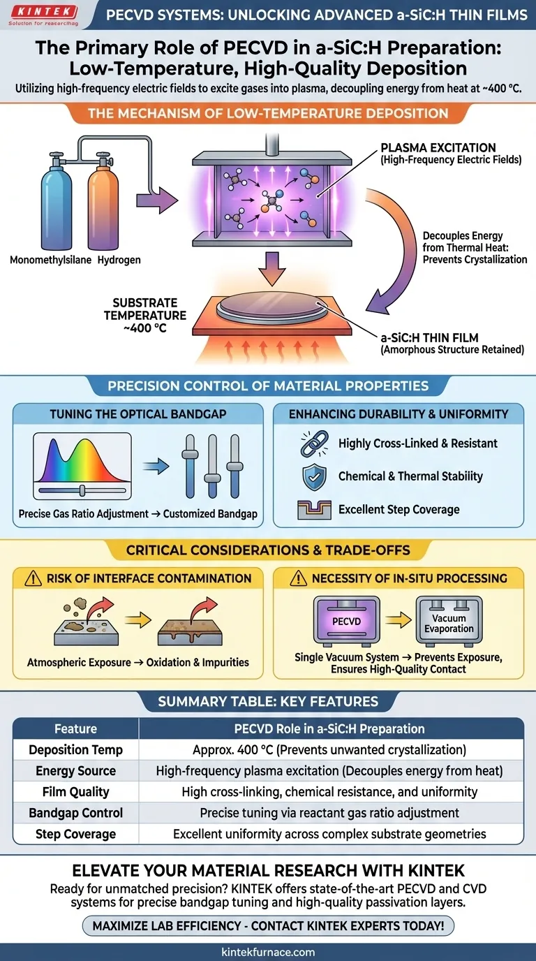
The primary role of Plasma Enhanced Chemical Vapor Deposition (PECVD) systems in the preparation of hydrogenated amorphous silicon carbide (a-SiC:H) is to facilitate chemical deposition at significantly reduced substrate temperatures. By utilizing high-frequency electric fields to excite reactant gases—specifically monomethylsilane and hydrogen—into a plasma state, PECVD allows for the creation of high-quality thin films at approximately 400 °C. This process is fundamental to fabricating wide-bandgap passivation layers that require precise compositional control without the thermal stress of traditional methods.
PECVD systems are indispensable for a-SiC:H preparation because they decouple reaction energy from thermal heat, allowing for the precise tuning of optical bandgaps and film composition while maintaining the essential amorphous structure of the material.
The Mechanism of Low-Temperature Deposition
Plasma Excitation
PECVD systems function by applying high-frequency electric fields to reactant gases. This energy excites the gas molecules, transforming them into a plasma state.
Reducing Thermal Requirements
Because the plasma provides the energy necessary to drive chemical reactions, the substrate does not need to be heated to extreme temperatures.
Maintaining Amorphous Structure
The ability to operate at approximately 400 °C is critical for a-SiC:H films. This temperature range ensures the material retains its amorphous structure rather than crystallizing, which is often required for specific optical and electronic applications.
Precision Control of Material Properties
Tuning the Optical Bandgap
The primary advantage of using PECVD for a-SiC:H is the ability to manipulate the film's composition. Operators can precisely adjust the optical bandgap of the resulting thin film, making it an ideal choice for passivation layers.
Enhancing Physical Durability
Films deposited via PECVD generally exhibit excellent physical characteristics. They are typically highly cross-linked, uniform, and resistant to both chemical and thermal changes.
Uniformity and Coverage
Beyond composition, PECVD systems are noted for providing excellent step coverage. This ensures that the film deposition is highly uniform across the substrate, which is vital for consistent device performance.
Critical Considerations and Trade-offs
The Risk of Interface Contamination
While PECVD offers excellent control, the quality of the film is highly sensitive to the deposition environment. If a sample is exposed to the atmosphere between the deposition of different layers (such as a base and a capping layer), oxidation and contamination can occur.
The Necessity of In-Situ Processing
To mitigate contamination risks, it is often necessary to integrate PECVD within a single vacuum system alongside other technologies. This "in-situ" approach prevents atmospheric exposure, ensuring high-quality physical contact between layers, such as germanium nanocrystals and the silicon carbide matrix.
Making the Right Choice for Your Goal
To maximize the effectiveness of PECVD for your specific application, consider the following:
- If your primary focus is optical performance: Prioritize the precise control of reactant gas ratios to tune the optical bandgap while maintaining the substrate at 400 °C.
- If your primary focus is multi-layer device integration: Utilize an in-situ system that combines PECVD with vacuum evaporation to prevent interface oxidation and ensure high-quality contact between layers.
Leveraging PECVD effectively requires balancing the need for low-temperature processing with the strict requirement for environmental control during deposition.
Summary Table:
| Feature | PECVD Role in a-SiC:H Preparation |
|---|---|
| Deposition Temp | Approx. 400 °C (Prevents unwanted crystallization) |
| Energy Source | High-frequency plasma excitation (Decouples energy from heat) |
| Film Quality | High cross-linking, chemical resistance, and uniformity |
| Bandgap Control | Precise tuning via reactant gas ratio adjustment |
| Step Coverage | Excellent uniformity across complex substrate geometries |
Elevate Your Material Research with KINTEK
Ready to achieve unmatched precision in your thin-film deposition? KINTEK offers state-of-the-art PECVD and CVD systems, alongside our extensive range of customizable lab furnaces. Backed by expert R&D and world-class manufacturing, we provide the tools needed for precise bandgap tuning and high-quality passivation layers.
Maximize your lab's efficiency and ensure superior device performance—Contact KINTEK experts today to find your perfect deposition solution!
Visual Guide
References
- Z. Remeš, Oleg Babčenko. Thin Hydrogenated Amorphous Silicon Carbide Layers with Embedded Ge Nanocrystals. DOI: 10.3390/nano15030176
This article is also based on technical information from Kintek Furnace Knowledge Base .
Related Products
- RF PECVD System Radio Frequency Plasma Enhanced Chemical Vapor Deposition
- Slide PECVD Tube Furnace with Liquid Gasifier PECVD Machine
- Inclined Rotary Plasma Enhanced Chemical Deposition PECVD Tube Furnace Machine
- Inclined Rotary Plasma Enhanced Chemical Deposition PECVD Tube Furnace Machine
- 915MHz MPCVD Diamond Machine Microwave Plasma Chemical Vapor Deposition System Reactor
People Also Ask
- How are deposition rates and film properties controlled in PECVD? Master Key Parameters for Optimal Thin Films
- What are the system specifications of the PECVD system? Unlock Precision Thin-Film Deposition
- What are the advantages of PECVD in film deposition? Achieve Low-Temp, High-Quality Coatings
- What are some promising applications of PECVD-prepared 2D materials? Unlock Advanced Sensing and Optoelectronics
- What are the limitations of PECVD? Overcome Process Control and Cost Challenges


