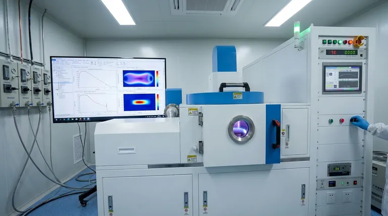
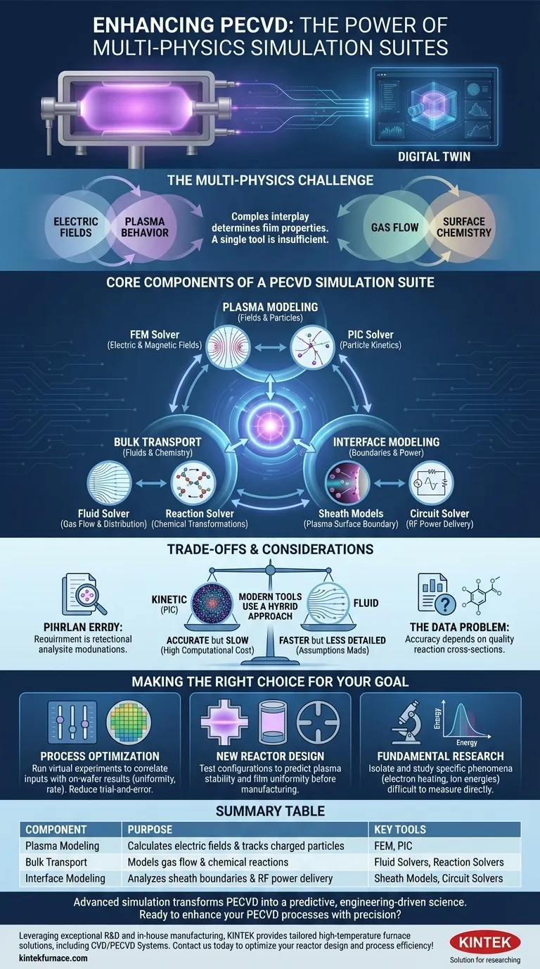
The short answer is that Plasma-Enhanced Chemical Vapor Deposition (PECVD) is not enhanced by a single tool, but by sophisticated, multi-physics simulation suites. These platforms integrate multiple specialized solvers to create a "digital twin" of the reactor, modeling everything from the plasma physics and gas chemistry to the electrical circuits delivering power.
To truly enhance a PECVD process, simulation must move beyond modeling isolated phenomena. The goal is to capture the complex interplay between the electric fields, plasma behavior, gas flow, and surface chemistry that collectively determine the final film properties.
Why PECVD Simulation is a Multi-Physics Challenge
A PECVD reactor is an intricate environment where multiple physical domains overlap and influence one another. Optimizing a process requires understanding how a change in one parameter, like RF power, cascades through the entire system to affect film uniformity and quality.
This is why a single, simple simulation is insufficient. Effective tools must simultaneously solve for the electromagnetics driving the plasma, the motion of individual ions and electrons, the bulk flow of gases, and the chemical reactions happening both in the gas phase and on the substrate surface.
The Core Components of a PECVD Simulation Suite
A comprehensive PECVD simulation tool is best understood as a suite of interconnected modules. Each module is responsible for a specific piece of the physics.
Modeling the Plasma: Fields and Particles
The heart of a PECVD reactor is the plasma. Its behavior is governed by the interaction of electric fields and charged particles.
A Finite Element Method (FEM) solver is used to calculate the electric and magnetic fields throughout the chamber. These fields are the invisible forces that energize and direct the plasma.
A Particle-in-Cell (PIC) solver then tracks the kinetic motion of individual charged particles, like ions and electrons, as they are accelerated by these fields. This provides a highly accurate, fundamental view of particle energy and distribution.
Modeling Bulk Transport: Fluids and Chemistry
While a PIC model is great for charged particles, it's too computationally expensive for the vast number of neutral gas molecules.
A fluid solver is used to model the bulk movement of precursor gases into the chamber and reaction byproducts out of it. This is critical for understanding gas distribution and ensuring uniform delivery to the substrate.
A reaction solver models the crucial chemical transformations. It calculates how electron collisions break apart precursor gases and simulates the subsequent chain of gas-phase and surface reactions that ultimately lead to film deposition.
Modeling the Critical Interfaces
The connection between the simulation and the real world depends on accurately modeling the system's boundaries.
Complex sheath models are essential for understanding the thin boundary layer between the bulk plasma and the substrate. The sheath controls the energy and angle at which ions strike the surface, which directly impacts film density, stress, and quality.
A circuit solver models the external RF power delivery system. This ensures that the power and voltage specified in the simulation accurately reflect what the plasma inside the chamber actually experiences, closing the loop between the equipment and the process.
Understanding the Trade-offs: Complexity vs. Speed
The primary challenge in PECVD simulation is managing computational complexity. A full-system model that includes all the components described above can be incredibly demanding.
Kinetic vs. Fluid Models
The most significant trade-off is between kinetic (PIC) and fluid plasma models. PIC models are fundamentally accurate but extremely slow, often limited to simulating small domains or short time scales.
Fluid models are much faster but make assumptions about particle energy distributions. Many modern tools use a hybrid approach, applying kinetic models only where necessary (like in the sheaths) and fluid models for the bulk plasma to achieve a balance of accuracy and speed.
The Data Problem
The accuracy of any reaction solver is entirely dependent on the quality of its input data, specifically the reaction cross sections. This data, which defines the probability of a specific chemical reaction occurring, can be difficult to find or measure experimentally, often representing the weakest link in the simulation chain.
Making the Right Choice for Your Goal
Using these powerful simulation suites effectively means aligning the simulation's complexity with your specific objective.
- If your primary focus is process optimization: Use simulation to run virtual experiments, correlating inputs like power and pressure with on-wafer results like uniformity and deposition rate, reducing costly trial-and-error on actual hardware.
- If your primary focus is new reactor design: Employ simulation to test different chamber geometries, gas inlet configurations, and electrode designs to predict plasma stability and film uniformity before committing to manufacturing.
- If your primary focus is fundamental research: Leverage detailed kinetic models to isolate and study specific phenomena, such as electron heating mechanisms or ion energy distributions, that are difficult or impossible to measure directly.
Ultimately, advanced simulation transforms PECVD from a "black box" art into a predictive, engineering-driven science.
Summary Table:
| Simulation Component | Purpose | Key Tools |
|---|---|---|
| Plasma Modeling | Calculates electric fields and tracks charged particles | FEM, PIC |
| Bulk Transport | Models gas flow and chemical reactions | Fluid Solvers, Reaction Solvers |
| Interface Modeling | Analyzes sheath boundaries and RF power delivery | Sheath Models, Circuit Solvers |
Ready to enhance your PECVD processes with precision? Leveraging exceptional R&D and in-house manufacturing, KINTEK provides diverse laboratories with advanced high-temperature furnace solutions, including CVD/PECVD Systems. Our strong deep customization capability ensures we can precisely meet your unique experimental requirements. Contact us today to discuss how our tailored solutions can optimize your reactor design and process efficiency!
Visual Guide
Related Products
- RF PECVD System Radio Frequency Plasma Enhanced Chemical Vapor Deposition
- Slide PECVD Tube Furnace with Liquid Gasifier PECVD Machine
- Inclined Rotary Plasma Enhanced Chemical Deposition PECVD Tube Furnace Machine
- Inclined Rotary Plasma Enhanced Chemical Deposition PECVD Tube Furnace Machine
- Cylindrical Resonator MPCVD Machine System for Lab Diamond Growth
People Also Ask
- What is the role of RF power in PECVD and how does the RF-PECVD process work? Master Thin Film Deposition Control
- What is PECVD specification? A Guide to Choosing the Right System for Your Lab
- What are some promising applications of PECVD-prepared 2D materials? Unlock Advanced Sensing and Optoelectronics
- What is RF in PECVD? A Critical Control for Plasma Deposition
- How are deposition rates and film properties controlled in PECVD? Master Key Parameters for Optimal Thin Films


