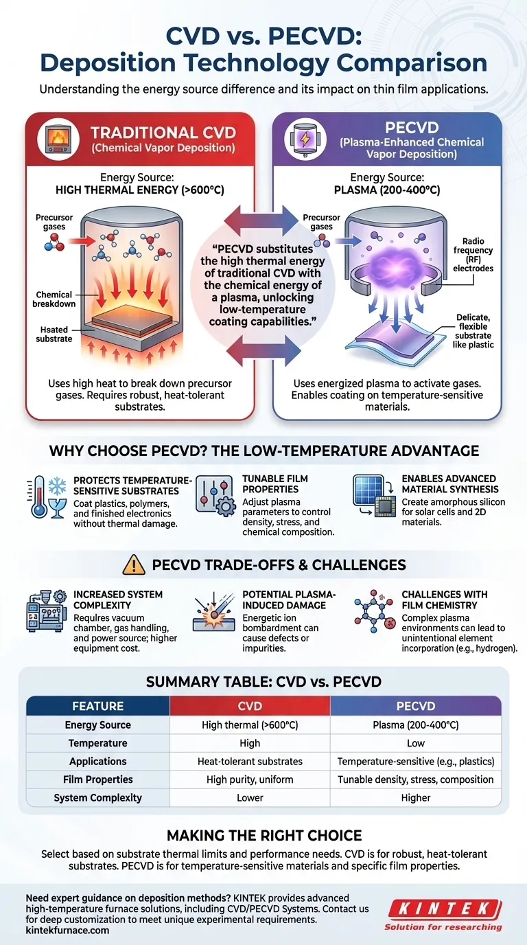
At its core, Plasma-Enhanced Chemical Vapor Deposition (PECVD) is a process for depositing thin films that uses an energized gas, or plasma, to drive the chemical reaction. Unlike conventional Chemical Vapor Deposition (CVD), which relies almost exclusively on high heat to break down precursor gases, PECVD uses this plasma to create highly reactive molecules at much lower temperatures. This fundamental difference makes it suitable for entirely different applications.
The central takeaway is that PECVD substitutes the high thermal energy of traditional CVD with the chemical energy of a plasma. This unlocks the ability to coat temperature-sensitive materials but introduces new trade-offs related to equipment complexity and potential film damage.
The Fundamental Difference: Energy Source
The choice between CVD and PECVD comes down to how you provide the energy needed to transform a gas into a solid film on your substrate.
How Traditional CVD Works: The Thermal Approach
Conventional CVD is conceptually simple. Precursor gases are introduced into a high-temperature furnace containing the substrate.
The intense heat (often >600°C) provides the thermal energy necessary to break the chemical bonds in the gas molecules. These newly reactive fragments then settle on the hot substrate surface and form the desired solid film.
How PECVD Works: The Plasma-Powered Approach
PECVD avoids the need for extreme heat by creating a plasma inside the reaction chamber using an electric field (like radio frequency or microwave energy).
This plasma is a highly energetic state of matter—a gas of ions, electrons, and reactive radicals. These energized particles can break down the precursor gases through collisions, creating the necessary reactive fragments without requiring a hot surface. The process can therefore run at significantly lower temperatures, typically 200-400°C.
Why Choose PECVD? The Low-Temperature Advantage
The primary driver for using PECVD is its ability to operate at low temperatures, which opens up capabilities that are impossible with high-temperature thermal CVD.
Protecting Temperature-Sensitive Substrates
This is the most critical advantage of PECVD. Many materials, such as plastics, polymers, or semiconductor wafers with pre-existing metallic layers, cannot withstand the high temperatures of traditional CVD.
PECVD allows for the deposition of high-quality films like silicon dioxide or silicon nitride onto these sensitive substrates without damaging them.
Achieving Different Film Properties
The energy of the plasma can be controlled independently of temperature. This gives engineers an additional "knob" to turn.
By adjusting plasma power, pressure, and gas chemistry, one can tune the final film's properties, such as its density, internal stress, and chemical composition.
Enabling Advanced Material Synthesis
PECVD facilitates the creation of materials that are difficult to produce otherwise. For example, it is used to deposit amorphous silicon for solar cells and thin-film transistors.
It also enables cleaner, catalyst-free production of advanced 2D materials by providing precise control over the reaction environment.
Understanding the Trade-offs
While powerful, the use of plasma is not without its costs. Choosing PECVD involves accepting a specific set of engineering challenges.
Increased System Complexity
A PECVD system requires a vacuum chamber, gas handling, and a power source (e.g., an RF generator) with a matching network to create and sustain the plasma. This makes the equipment more complex and expensive than a standard CVD furnace.
Potential for Plasma-Induced Damage
The energetic ions within the plasma can bombard the substrate and the growing film. This bombardment can be beneficial, helping to densify the film, but it can also cause defects, impurities, or high compressive stress if not properly controlled.
Challenges with Film Chemistry
Plasma environments are chemically very complex. The precursor gases can fragment in multiple ways, sometimes leading to the unintentional incorporation of elements like hydrogen into the film, which can affect its electronic or optical properties.
Making the Right Choice for Your Goal
Your choice depends entirely on your substrate's limitations and your final performance requirements.
- If your primary focus is coating a robust, heat-tolerant substrate: Traditional CVD is often a simpler, more cost-effective method that yields high-purity, uniform films.
- If your primary focus is coating a temperature-sensitive material like plastic or a finished electronic device: PECVD is often the only viable option due to its low-temperature processing capability.
- If your primary focus is achieving a specific film density or stress level at a high deposition rate: PECVD provides more control parameters to tune the film's properties, but requires more extensive process development.
Ultimately, selecting the right deposition method requires balancing your material's thermal budget against the desired film characteristics and acceptable system complexity.
Summary Table:
| Feature | CVD | PECVD |
|---|---|---|
| Energy Source | High thermal energy (>600°C) | Plasma (200-400°C) |
| Temperature | High | Low |
| Applications | Heat-tolerant substrates | Temperature-sensitive materials (e.g., plastics, electronics) |
| Film Properties | High purity, uniform | Tunable density, stress, composition |
| System Complexity | Lower | Higher |
Need expert guidance on choosing the right deposition method for your lab? Leveraging exceptional R&D and in-house manufacturing, KINTEK provides diverse laboratories with advanced high-temperature furnace solutions, including CVD/PECVD Systems. Our strong deep customization capability ensures we precisely meet your unique experimental requirements. Contact us today to enhance your thin film processes with tailored solutions!
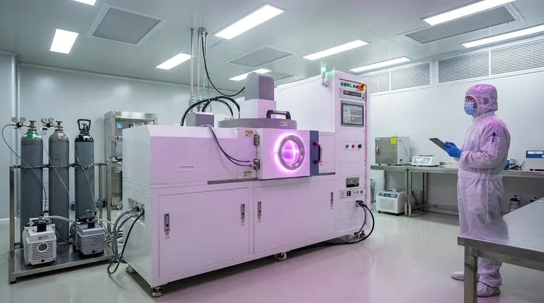
Visual Guide
Related Products
- RF PECVD System Radio Frequency Plasma Enhanced Chemical Vapor Deposition
- Slide PECVD Tube Furnace with Liquid Gasifier PECVD Machine
- Inclined Rotary Plasma Enhanced Chemical Deposition PECVD Tube Furnace Machine
- Inclined Rotary Plasma Enhanced Chemical Deposition PECVD Tube Furnace Machine
- Cylindrical Resonator MPCVD Machine System for Lab Diamond Growth
People Also Ask
- What is the role of RF power in PECVD and how does the RF-PECVD process work? Master Thin Film Deposition Control
- What are some promising applications of PECVD-prepared 2D materials? Unlock Advanced Sensing and Optoelectronics
- How are deposition rates and film properties controlled in PECVD? Master Key Parameters for Optimal Thin Films
- How is silicon dioxide deposited from tetraethylorthosilicate (TEOS) in PECVD? Achieve Low-Temperature, High-Quality SiO2 Films
- What is RF in PECVD? A Critical Control for Plasma Deposition


