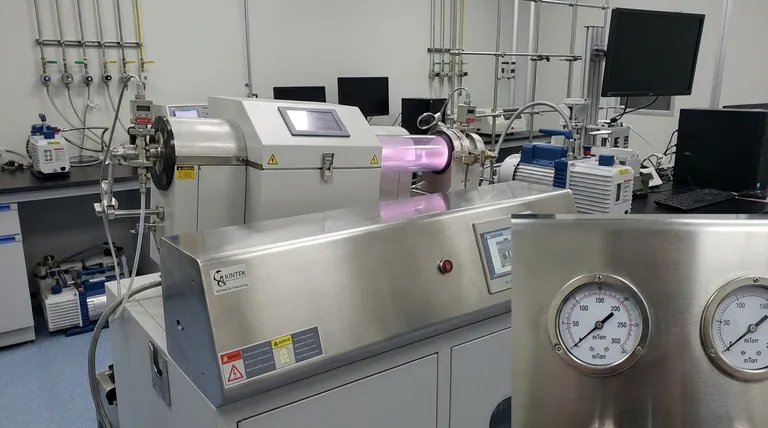
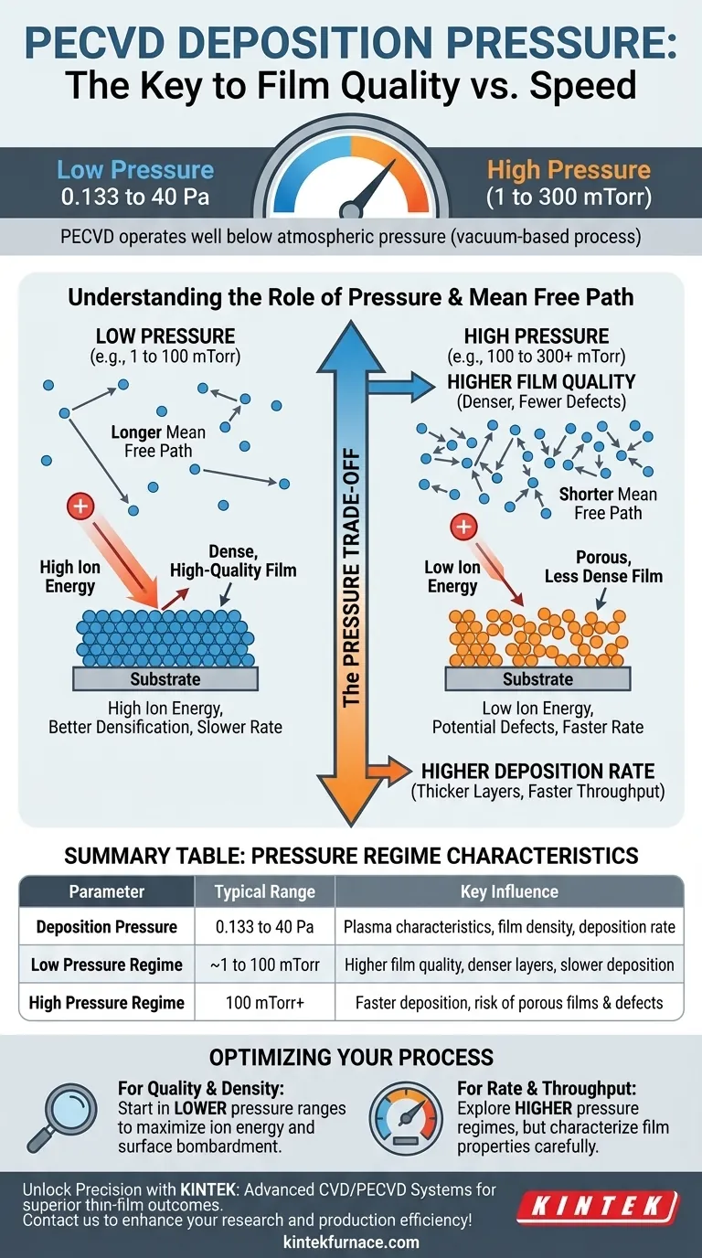
In a standard PECVD system, the typical deposition pressure ranges from 0.133 to 40 Pascals (Pa), which is equivalent to approximately 1 to 300 millitorr (mTorr). This operating window exists well below atmospheric pressure, classifying Plasma-Enhanced Chemical Vapor Deposition (PECVD) as a vacuum-based process. The exact pressure is a critical parameter that is carefully adjusted based on the specific material being deposited and the desired film properties.
Pressure is not merely a background condition in PECVD; it is a primary control lever. The choice of pressure directly governs the plasma's characteristics, forcing a fundamental trade-off between the speed of deposition and the ultimate quality and density of the thin film.
The Role of Pressure in a PECVD System
To understand why this specific pressure range is used, we must look at how it influences the core mechanics of the PECVD process. It's a delicate balance between having enough material to deposit and enough space for the plasma to function effectively.
Establishing a Controlled Vacuum Environment
Like traditional Chemical Vapor Deposition (CVD), PECVD is a vacuum deposition method. The process chamber is pumped down to a low base pressure to remove contaminants like oxygen and water vapor, which could interfere with the film chemistry.
The precursor gases are then introduced, and the pressure is stabilized within the operational range (e.g., 0.133 to 40 Pa). This ensures the precursor gases are the dominant species in the chamber, leading to higher-purity films.
Creating and Sustaining the Plasma
Plasma is an ionized gas containing a mix of ions, electrons, radicals, and neutral molecules. In PECVD, an electric field energizes the precursor gases to create this plasma.
The pressure determines the density of gas molecules in the chamber. There must be enough molecules to sustain the plasma discharge but not so many that the plasma becomes unstable or inefficient.
The Concept of Mean Free Path
The most critical concept pressure controls is the mean free path: the average distance a particle (like an electron or ion) travels before colliding with another particle.
At lower pressures, the mean free path is longer. Electrons can accelerate to higher energies before a collision, leading to more efficient ionization and dissociation of precursor gases.
At higher pressures, the mean free path is shorter. Particles collide more frequently, which changes the energy distribution and the type of chemical reactions that occur.
How Pressure Influences Film Deposition
Adjusting the chamber pressure directly alters the mean free path, which in turn has a profound impact on both the deposition rate and the final properties of the film.
Impact on Deposition Rate
A higher operating pressure generally increases the concentration of reactant species in the chamber. This can lead to a higher deposition rate, as more film-forming precursors are available to react on the substrate surface.
However, this relationship is not linear. Deposition rate is also heavily dependent on gas flow rates and plasma power.
Impact on Film Quality and Density
Lower pressure and a longer mean free path allow ions to accelerate to higher energies before striking the substrate. This high-energy bombardment transfers momentum to the growing film.
This "atomic peening" effect results in a denser, more compact film with lower porosity. This is often desirable for creating high-quality optical or electronic layers.
Conversely, higher pressures lead to lower-energy ion bombardment, which can result in less dense and more porous films.
Understanding the Trade-offs
The choice of pressure is always a balance between competing goals. There is no single "best" pressure; it depends entirely on the process objective.
Low-Pressure Regimes (~1 to 100 mTorr)
Operating at the lower end of the pressure range favors the creation of high-quality films. The high ion energy promotes surface mobility and densification.
The primary trade-off is often a slower deposition rate. This may not be suitable for applications requiring thick films or high throughput.
High-Pressure Regimes (~100 mTorr to a few Torr)
Higher pressures can significantly increase deposition rates by increasing reactant density and gas-phase collisions.
The risk is a reduction in film quality. It can lead to more porous films and may even cause gas-phase nucleation, where particles form in the plasma itself and fall onto the substrate, creating defects.
Pressure vs. Other Parameters
Pressure never works in isolation. It is part of a multi-variable system that includes plasma power, gas flow rate, and temperature. For example, a high deposition rate might be achieved at low pressure by significantly increasing the plasma power or gas flow. Fine-tuning a process requires adjusting these parameters in concert.
Making the Right Choice for Your Goal
The optimal pressure setting is dictated by the primary goal of your deposition process.
- If your primary focus is high-quality, dense, low-defect films: Start your process development in a lower pressure range to maximize ion energy and surface bombardment.
- If your primary focus is a high deposition rate for thicker layers: Explore higher pressure regimes, but be sure to characterize the film for properties like porosity, stress, and purity to ensure it still meets your minimum requirements.
Mastering the role of pressure is fundamental to moving from simply running a PECVD process to truly engineering its outcome.
Summary Table:
| Parameter | Typical Range | Key Influence |
|---|---|---|
| Deposition Pressure | 0.133 to 40 Pa (1-300 mTorr) | Controls plasma characteristics, film density, and deposition rate |
| Low Pressure (1-100 mTorr) | ~0.133 to 13.3 Pa | Higher film quality, denser layers, slower deposition |
| High Pressure (100 mTorr+) | >13.3 Pa | Faster deposition, risk of porous films and defects |
Unlock Precision in Your PECVD Processes with KINTEK
Struggling to balance film quality and deposition speed in your lab? KINTEK specializes in advanced high-temperature furnace solutions, including our customizable CVD/PECVD Systems. Leveraging exceptional R&D and in-house manufacturing, we provide tailored equipment to meet your unique experimental needs—ensuring optimal pressure control for superior thin-film outcomes. Contact us today to discuss how our expertise can enhance your research and production efficiency!
Visual Guide
Related Products
- Slide PECVD Tube Furnace with Liquid Gasifier PECVD Machine
- Inclined Rotary Plasma Enhanced Chemical Deposition PECVD Tube Furnace Machine
- Inclined Rotary Plasma Enhanced Chemical Deposition PECVD Tube Furnace Machine
- RF PECVD System Radio Frequency Plasma Enhanced Chemical Vapor Deposition
- Multi Heating Zones CVD Tube Furnace Machine for Chemical Vapor Deposition Equipment
People Also Ask
- What plasma source is used in PE-CVD tube furnaces? Unlock Low-Temperature, High-Quality Deposition
- How does PECVD equipment contribute to TOPCon bottom cells? Mastering Hydrogenation for Maximum Solar Efficiency
- What is plasma in the context of PECVD? Unlock Low-Temperature Thin Film Deposition
- In which industries is the tube furnace commonly used? Essential for Materials Science, Energy, and More
- What role does a Tube Furnace play in the CVD growth of carbon nanotubes? Achieve High-Purity CNT Synthesis


