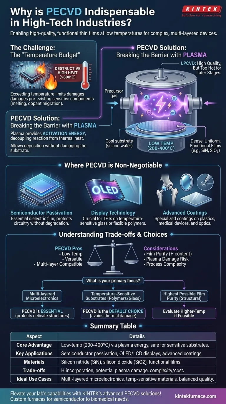
In modern high-tech manufacturing, Plasma-Enhanced Chemical Vapor Deposition (PECVD) is considered indispensable because it uniquely allows for the creation of high-quality, functional thin films at low temperatures. This capability is critical for building complex, multi-layered devices, as it avoids damaging sensitive components that have already been fabricated. Its versatility in depositing different materials makes it a cornerstone process in fields from semiconductors to biomedical devices.
The central challenge in advanced manufacturing is adding new layers to a device without destroying the work already done. PECVD solves this by using the energy from a plasma, rather than destructive high heat, to drive the chemical reactions needed to form a new film.
The Core Problem: The "Temperature Budget"
What is a Temperature Budget?
In fabricating a device like a microchip, each processing step has a maximum temperature it can tolerate. This is known as the temperature budget.
Exceeding this budget, even for a short time, can cause irreversible damage, such as melting structures, altering material properties, or causing meticulously placed atoms (dopants) to move, ruining the device's function.
The Limits of High-Heat Methods
Traditional methods like Low-Pressure Chemical Vapor Deposition (LPCVD) create exceptionally high-quality films, but they require very high temperatures (often >600°C).
This heat is simply not an option for later-stage fabrication steps. You cannot deposit a final protective layer on a completed microchip at 600°C without destroying the billions of transistors underneath.
How PECVD Breaks the Temperature Barrier
The Role of Plasma
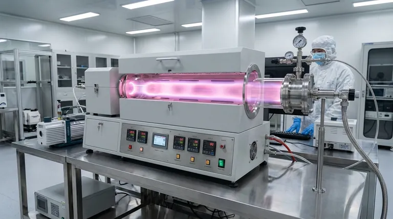
PECVD's key innovation is the use of plasma, an energized state of gas created by an electromagnetic field. Think of it as a controlled, miniature lightning storm inside a vacuum chamber.
This plasma is filled with high-energy electrons that collide with the precursor gas molecules.
Driving Reactions Without Heat
The energy from these electron collisions is what breaks the precursor gases apart, providing the chemical energy needed for the deposition reaction.
Because the plasma provides the activation energy, the substrate itself does not need to be heated to extreme temperatures. PECVD processes typically run at much lower temperatures, usually between 200°C and 400°C.
The Result: High-Quality Films on Sensitive Substrates
This low-temperature capability allows engineers to deposit dense, uniform, and functional films—such as silicon nitride (SiN) or silicon dioxide (SiO2)—directly onto fully formed devices or temperature-sensitive materials like plastic.
Where PECVD is Non-Negotiable
Semiconductor Passivation
After transistors are built, they need a final, protective insulating layer (passivation). PECVD is the only practical way to deposit this dielectric film without degrading the performance of the underlying circuitry.
Display Technology
Modern OLED and LCD screens are built on large glass or even flexible polymer substrates. These materials cannot withstand high temperatures. PECVD is essential for creating the thin-film transistors (TFTs) that control each pixel.
Advanced Coatings
PECVD is used to apply specialized coatings on products that cannot be heated. This includes hard, scratch-resistant films on plastics, biocompatible layers on medical implants, and anti-reflective coatings on optical components.
Understanding the Trade-offs
Film Purity and Composition
While PECVD films are excellent for their intended purpose, they often contain hydrogen, which is incorporated from the precursor gases. For some highly specific applications, the ultra-pure films from high-temperature LPCVD may still be superior if the temperature budget allows.
Potential for Plasma Damage
The same energetic ions that drive the reaction can, if not properly controlled, physically bombard and damage the substrate surface. Modern PECVD systems are highly engineered to minimize this effect, but it remains a fundamental consideration of the process.
Process Complexity
Generating a stable, uniform plasma across a large substrate (like a 300mm silicon wafer) is a significant engineering challenge. PECVD reactors are complex and expensive machines that require precise control over gas flow, pressure, and RF power.
Making the Right Choice for Your Goal
PECVD is a foundational tool, but its application depends on your specific constraints and objectives.
- If your primary focus is fabricating multi-layered microelectronics: PECVD is essential for depositing insulating or protective layers without disturbing the delicate transistor structures underneath.
- If your primary focus is coating temperature-sensitive substrates (like polymers or glass): PECVD is the default choice, as it avoids the thermal damage inherent in conventional deposition methods.
- If your primary focus is achieving the highest possible film purity for a structural layer: You should evaluate if a higher-temperature process is feasible, but for most modern electronic applications, PECVD provides the necessary balance of quality and compatibility.
Ultimately, PECVD's unique ability to decouple reaction energy from thermal energy is the fundamental reason it remains a cornerstone of advanced technological innovation.
Summary Table:
| Aspect | Details |
|---|---|
| Core Advantage | Low-temperature deposition (200-400°C) using plasma energy, avoiding damage to sensitive substrates |
| Key Applications | Semiconductor passivation, display technology (OLED/LCD), advanced coatings (e.g., scratch-resistant, biocompatible) |
| Materials Deposited | Silicon nitride (SiN), silicon dioxide (SiO2), and other functional thin films |
| Trade-offs | Potential hydrogen incorporation in films, risk of plasma damage, and higher process complexity and cost |
| Ideal Use Cases | Multi-layered microelectronics, temperature-sensitive substrates (polymers, glass), where high purity is balanced with thermal constraints |
Elevate your lab's capabilities with KINTEK's advanced PECVD solutions! Leveraging exceptional R&D and in-house manufacturing, we provide diverse laboratories with high-temperature furnace systems like CVD/PECVD, Muffle, Tube, Rotary, Vacuum & Atmosphere Furnaces. Our strong deep customization capability ensures precise alignment with your unique experimental needs, from semiconductor fabrication to biomedical coatings. Contact us today to discuss how our tailored solutions can enhance your research and production efficiency!
Visual Guide
Related Products
- Slide PECVD Tube Furnace with Liquid Gasifier PECVD Machine
- RF PECVD System Radio Frequency Plasma Enhanced Chemical Vapor Deposition
- Inclined Rotary Plasma Enhanced Chemical Deposition PECVD Tube Furnace Machine
- Inclined Rotary Plasma Enhanced Chemical Deposition PECVD Tube Furnace Machine
- Multi Heating Zones CVD Tube Furnace Machine for Chemical Vapor Deposition Equipment
People Also Ask
- What is plasma in the context of PECVD? Unlock Low-Temperature Thin Film Deposition
- How does PECVD equipment contribute to TOPCon bottom cells? Mastering Hydrogenation for Maximum Solar Efficiency
- What are the main advantages of PECVD tube furnaces compared to CVD tube furnaces? Lower Temp, Faster Deposition, and More
- What are the disadvantages of tube furnace cracking when processing heavy raw materials? Avoid Costly Downtime and Inefficiency
- What are the advantages of using a tube furnace CVD system for Cu(111)/graphene? Superior Scalability and Quality


