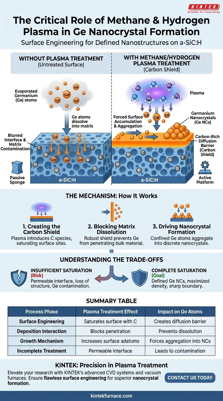
Methane and hydrogen plasma treatment acts as a critical surface engineering step to enable nanostructure growth. By exposing the hydrogenated amorphous silicon carbide (a-SiC:H) surface to this specific plasma environment, you saturate the surface with carbon atoms. This process effectively creates a chemical shield that prevents subsequently deposited germanium from dissolving into the underlying matrix, forcing it to organize into discrete nanocrystals instead.
The plasma treatment creates a carbon-rich diffusion barrier on the a-SiC:H surface. This barrier physically blocks germanium atoms from penetrating the underlying matrix, compelling them to accumulate on the surface and aggregate into stable nanocrystal structures.

The Mechanism of Surface Saturation
Creating the Carbon Shield
The primary function of the methane and hydrogen plasma is to alter the surface chemistry of the a-SiC:H. The plasma introduces carbon species that bond with and saturate the surface sites of the substrate. This results in a distinct, carbon-rich layer sitting atop the bulk material.
Blocking Matrix Dissolution
Without this specific treatment, the interface between germanium and a-SiC:H is permeable. Evaporated germanium atoms naturally tend to diffuse downward and dissolve into the amorphous silicon carbide matrix. The carbon-saturated layer acts as a robust diffusion barrier, effectively closing off this migration pathway.
Driving Nanocrystal Formation
Forcing Surface Accumulation
Because the germanium atoms are blocked from entering the bulk material, they are confined to the surface. This confinement drastically increases the concentration of germanium adatoms on top of the carbon barrier.
Promoting Aggregation
With nowhere to go but the surface, the germanium atoms are thermodynamically driven to bond with one another. This forced interaction promotes the aggregation of atoms. Consequently, rather than forming a flat alloy or dissolving, the material self-assembles into distinct, discrete germanium nanocrystals (Ge NCs).
Understanding the Trade-offs
The Risk of Insufficient Saturation
The success of this process relies entirely on the integrity of the diffusion barrier. If the plasma treatment is too brief or the carbon saturation is incomplete, the barrier will fail.
Loss of Structural Definition
In the absence of a complete barrier, germanium atoms will revert to their natural tendency to diffuse into the matrix. This leads to a loss of distinct nanocrystal features and results in germanium contamination within the a-SiC:H layer rather than the desired surface structures.
Making the Right Choice for Your Goal
To maximize the effectiveness of your germanium deposition, apply the following principles:
- If your primary focus is maximizing nanocrystal density: Ensure the plasma treatment is sufficient to fully saturate the surface, as any gaps in carbon coverage will lead to material loss into the bulk.
- If your primary focus is interface definition: Utilize the methane/hydrogen plasma to create a sharp boundary between the substrate and the active germanium layer.
By utilizing this plasma treatment, you effectively convert the substrate from a passive sponge into an active platform that supports the self-assembly of defined nanostructures.
Summary Table:
| Process Phase | Plasma Treatment Effect | Impact on Ge Atoms |
|---|---|---|
| Surface Engineering | Saturates a-SiC:H surface with carbon atoms | Creates a robust chemical diffusion barrier |
| Deposition Interaction | Blocks penetration into the underlying matrix | Prevents dissolution and material loss into bulk |
| Growth Mechanism | Increases surface adatom concentration | Forces aggregation into discrete nanocrystals |
| Incomplete Treatment | Results in a permeable or weak interface | Leads to matrix contamination and loss of structure |
Elevate Your Nanostructure Engineering with KINTEK
Precision in plasma treatment is the key to unlocking superior germanium nanocrystal formation. At KINTEK, we understand that high-performance materials require exact environmental controls. Backed by expert R&D and world-class manufacturing, we provide advanced CVD systems, vacuum furnaces, and customizable high-temperature lab solutions designed to meet your most rigorous research needs.
Whether you are refining interface definition or maximizing nanocrystal density, KINTEK offers the specialized equipment to ensure your surface engineering is flawless. Contact us today to find the perfect system for your lab!
Visual Guide
References
- Z. Remeš, Oleg Babčenko. Thin Hydrogenated Amorphous Silicon Carbide Layers with Embedded Ge Nanocrystals. DOI: 10.3390/nano15030176
This article is also based on technical information from Kintek Furnace Knowledge Base .
Related Products
- HFCVD Machine System Equipment for Drawing Die Nano Diamond Coating
- Silicon Carbide SiC Thermal Heating Elements for Electric Furnace
- 915MHz MPCVD Diamond Machine Microwave Plasma Chemical Vapor Deposition System Reactor
- 1200℃ Controlled Inert Nitrogen Atmosphere Furnace
- 1400℃ Muffle Oven Furnace for Laboratory
People Also Ask
- What is Hot-filament Chemical Vapor Deposition (HFCVD)? Achieve High-Quality Thin Films with Precision Control
- What are the equipment for chemical vapor deposition? A Guide to the 5 Essential Components
- What is the significance of the vacuum pressure control system in the CVD coating process for powders?
- What is chemical vapor deposition (CVD) and its primary industrial application? Unlock Precision Thin Films for Electronics
- What role does Chemical Vapor Deposition (CVD) equipment play in the surface coating of carbon fibers for composites?