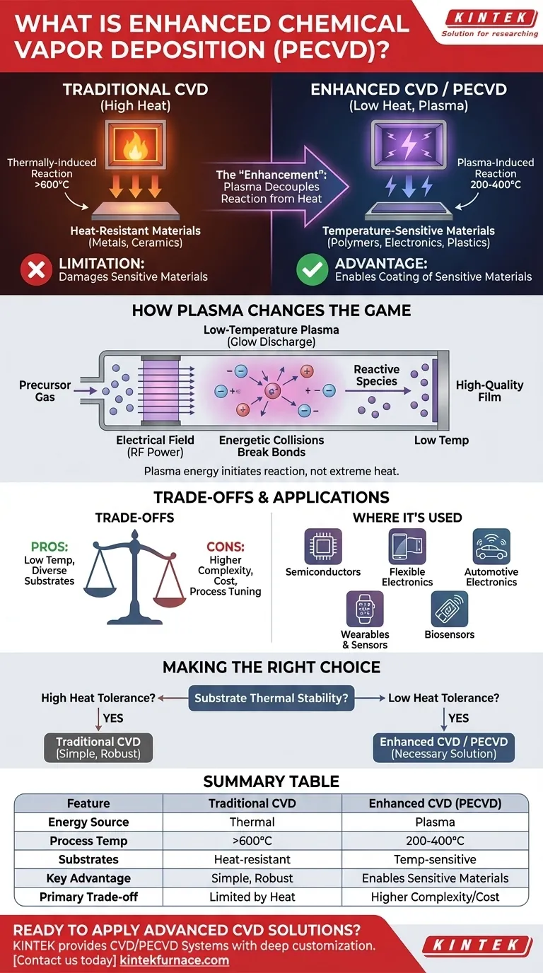
In essence, enhanced chemical vapor deposition refers to any advanced Chemical Vapor Deposition (CVD) process that uses an external energy source—other than just heat—to drive the coating reaction. The most common and important example is Plasma-Enhanced Chemical Vapor Deposition (PECVD), a technique that allows for high-quality thin films to be deposited at much lower temperatures than traditional methods.
The fundamental improvement of "enhanced" CVD is that it decouples the chemical reaction from high heat. By using energy from sources like plasma, it can create durable, high-performance coatings on temperature-sensitive materials that would be damaged or destroyed by conventional CVD processes.
Understanding the Foundation: Traditional CVD
The High-Temperature Reaction
Traditional Chemical Vapor Deposition (CVD) is a process for producing robust, thin-film coatings inside a vacuum chamber. It works by introducing gaseous precursor materials that are then subjected to high heat.
This heat triggers a thermally-induced chemical reaction, causing the precursors to decompose and deposit a solid, thin layer of material onto a substrate atom by atom.
The Inherent Limitation
The critical dependency of traditional CVD is high temperature. While effective, this requirement prevents its use on many modern materials, such as polymers, plastics, and complex electronic components that cannot withstand the intense heat without deforming or failing.
The "Enhancement": How Plasma Changes the Game
Introducing PECVD
Plasma-Enhanced Chemical Vapor Deposition (PECVD) is the leading form of enhanced CVD. It was developed specifically to overcome the temperature limitations of the traditional process.
The core principle of PECVD is to use energy from a plasma field, rather than just thermal energy, to initiate the chemical reaction needed for deposition.
The Role of Energized Plasma
In the PECVD process, an electrical field is used to ionize the precursor gases within the chamber, creating a low-temperature plasma (often seen as a glow discharge).
This plasma contains highly energetic electrons and ions that collide with the precursor gas molecules. These collisions break the chemical bonds and create reactive species that can then form a high-quality film on the substrate surface, all without requiring extreme heat.
The Low-Temperature Advantage
The ability to deposit films at lower temperatures is the primary advantage of PECVD. This enhancement makes it possible to apply durable, high-performance coatings to a vast range of materials that are central to modern technology.
This includes semiconductors, flexible electronics, plastics, and sensors that would be otherwise incompatible with high-temperature deposition methods.
Understanding the Trade-offs
Added Process Complexity
While powerful, the primary trade-off of enhanced CVD is increased complexity and cost. A PECVD system requires more than just a furnace and a vacuum pump.
It necessitates sophisticated radio-frequency (RF) power supplies to generate the plasma, advanced gas-handling systems, and precise controls to manage the plasma's density and energy.
Material and Rate Considerations
The films created by PECVD can sometimes have different properties (like hydrogen content) compared to high-temperature CVD films, which must be managed for specific applications. Deposition rates can also vary, requiring careful process tuning to achieve desired thickness and throughput.
Where Enhanced CVD Is Used
The Backbone of Modern Electronics
PECVD is a cornerstone of the semiconductor industry. It's used to deposit the insulating and protective layers essential for manufacturing integrated circuits.
Advanced Sensors and Devices
The ability to coat sensitive components has made enhanced CVD critical for a wide range of devices.
Applications include automotive electronics, smart home security devices, consumer electronics like smartphones and wearables, HVAC sensors, and highly sensitive biosensors.
Making the Right Choice for Your Goal
Deciding between traditional and enhanced CVD methods comes down to the thermal stability of your substrate and your performance requirements.
- If your primary focus is coating heat-resistant materials (like metals or ceramics): Traditional thermal CVD can be a simpler, effective, and robust choice.
- If your primary focus is coating temperature-sensitive materials (like polymers, plastics, or assembled electronics): Enhanced CVD, specifically PECVD, is the necessary and definitive solution.
By leveraging plasma to overcome the heat barrier, enhanced CVD enables the creation of the advanced materials that power modern technology.
Summary Table:
| Feature | Traditional CVD | Enhanced CVD (PECVD) |
|---|---|---|
| Primary Energy Source | Thermal (High Heat) | Plasma (Electrical Field) |
| Typical Process Temperature | High (>600°C) | Low (200-400°C) |
| Suitable Substrates | Heat-resistant materials (metals, ceramics) | Temperature-sensitive materials (polymers, plastics, electronics) |
| Key Advantage | Simple, robust process | Enables coating of sensitive materials |
| Primary Trade-off | Limited by substrate heat tolerance | Higher system complexity and cost |
Ready to Apply Advanced CVD Solutions to Your Projects?
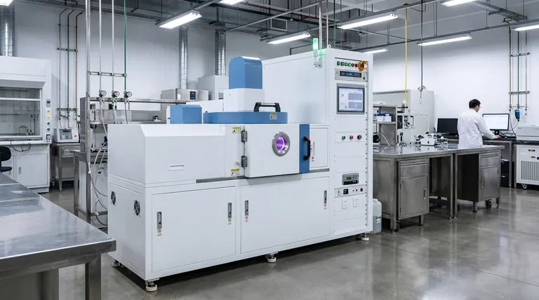
Leveraging exceptional R&D and in-house manufacturing, KINTEK provides diverse laboratories with advanced high-temperature furnace solutions. Our product line, including Tube Furnaces, Vacuum & Atmosphere Furnaces, and CVD/PECVD Systems, is complemented by our strong deep customization capability to precisely meet unique experimental requirements.
Whether you are developing next-generation semiconductors, flexible electronics, or sensitive biosensors, our expertise can help you achieve superior thin-film results. Contact us today to discuss how our tailored solutions can enhance your research and production!
Visual Guide
Related Products
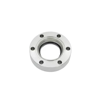
- RF PECVD System Radio Frequency Plasma Enhanced Chemical Vapor Deposition
- Slide PECVD Tube Furnace with Liquid Gasifier PECVD Machine
- MPCVD Machine System Reactor Bell-jar Resonator for Lab and Diamond Growth
- HFCVD Machine System Equipment for Drawing Die Nano Diamond Coating
- 915MHz MPCVD Diamond Machine Microwave Plasma Chemical Vapor Deposition System Reactor
People Also Ask
- What is the role of RF power in PECVD and how does the RF-PECVD process work? Master Thin Film Deposition Control
- What is PECVD specification? A Guide to Choosing the Right System for Your Lab
- What is RF in PECVD? A Critical Control for Plasma Deposition
- What are some promising applications of PECVD-prepared 2D materials? Unlock Advanced Sensing and Optoelectronics
- What are the key advantages of PECVD technology? Achieve Low-Temperature, High-Quality Thin Film Deposition