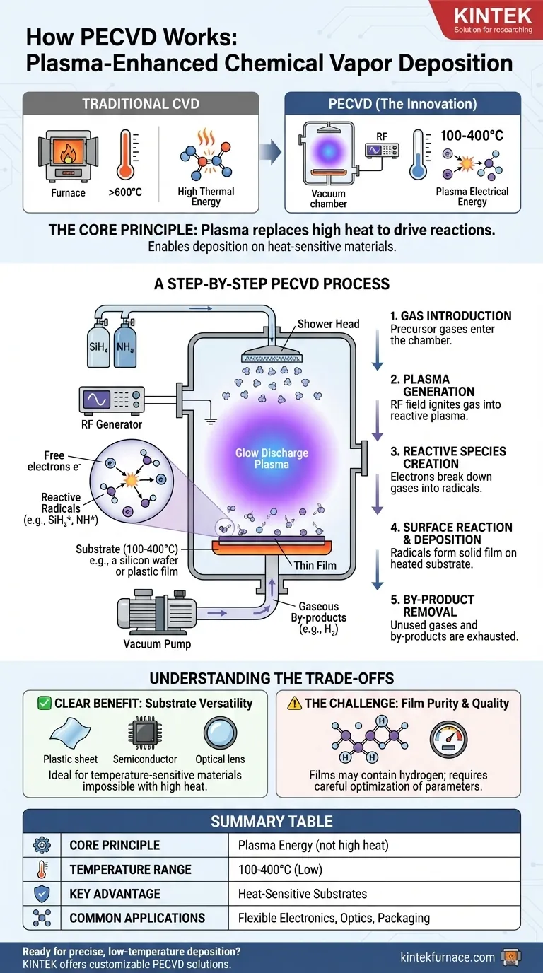
At its core, Plasma-Enhanced Chemical Vapor Deposition (PECVD) works by using an energized plasma to break down precursor gases into reactive species. Instead of relying solely on high temperatures, this plasma provides the necessary energy for chemical reactions to occur, allowing a thin film to form on a substrate at a much lower temperature than in traditional Chemical Vapor Deposition (CVD).
The fundamental difference in PECVD is its energy source. It substitutes the high thermal energy of conventional CVD with the electrical energy of a plasma, enabling high-quality film deposition on materials that cannot withstand intense heat.
The Core Principle: Plasma Instead of Heat
To understand how PECVD operates, you must first grasp its central concept: the replacement of thermal energy with plasma energy. This is the key innovation that defines the entire process.
What is Plasma in this Context?
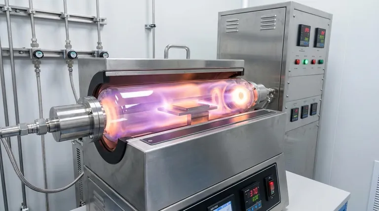
Plasma is often called the fourth state of matter. In a PECVD system, it is created by applying a strong radio frequency (RF) electric field to a low-pressure gas.
This field energizes the gas, stripping electrons from some of the gas molecules. The result is a highly reactive, ionized gas composed of ions, electrons, radicals, and neutral molecules.
How Plasma Drives the Reaction
In traditional CVD, high temperatures (often >600°C) are required to provide enough energy to break the chemical bonds of the precursor gases.
In PECVD, energetic electrons within the plasma collide with the stable precursor gas molecules. These collisions transfer energy, dissociating the molecules into chemically reactive radicals without requiring high ambient heat.
The Low-Temperature Advantage
These highly reactive radicals can then diffuse to the substrate surface and form the desired solid film at significantly lower temperatures, typically in the range of 100-400°C.
This makes PECVD invaluable for depositing films on substrates that would be damaged or destroyed by high temperatures, such as plastics, organic materials, or complex semiconductor devices with pre-existing metallic layers.
A Step-by-Step Breakdown of the PECVD Process
The operation of a PECVD system follows a clear, sequential process inside a vacuum chamber.
Step 1: Gas Introduction
Reactant gases, known as precursors, are introduced into the vacuum chamber. For example, to deposit silicon nitride (Si₃N₄), gases like silane (SiH₄) and ammonia (NH₃) are used.
These gases are often distributed evenly over the substrate through a perforated plate called a "shower head."
Step 2: Plasma Generation
An RF electric field (typically 100-300 eV) is applied between two electrodes inside the chamber, one of which is often the shower head.
This electrical discharge ignites the low-pressure gas mixture, creating a glow discharge plasma.
Step 3: Creation of Reactive Species
Free electrons in the plasma collide with and break down the stable precursor gas molecules. This creates a high concentration of chemically reactive radicals (e.g., SiH₂*, NH*).
Step 4: Surface Reaction and Deposition
These radicals diffuse to the heated substrate. On the surface, they undergo a series of chemical reactions, bonding with the surface and with each other to form a stable, solid thin film.
The substrate is gently heated to promote surface mobility and drive these reactions, ensuring a dense, high-quality film.
Step 5: By-product Removal
Gaseous by-products from the surface reactions (e.g., H₂) are removed from the chamber by the vacuum system, preventing them from being incorporated into the growing film.
Understanding the Trade-offs
No process is without its compromises. Understanding the trade-offs of PECVD is crucial for its effective application.
The Clear Benefit: Substrate Versatility
As emphasized, the primary advantage is the ability to deposit films on a wide variety of temperature-sensitive substrates. This opens up applications in flexible electronics, optics, and advanced semiconductor packaging that are impossible with high-temperature methods.
The Challenge: Film Quality and Purity
Because the deposition is not driven by thermal equilibrium, the resulting film properties can be more complex. For instance, PECVD silicon nitride films often contain a significant amount of hydrogen from the precursor gases.
This can affect the film's electrical properties, density, and stress. Controlling these properties requires careful optimization of multiple parameters, including RF power, gas flow rates, pressure, and temperature.
Making the Right Choice for Your Goal
Selecting a deposition method depends entirely on your project's constraints and desired outcome.
- If your primary focus is depositing films on heat-sensitive materials: PECVD is the industry-standard solution, as its low-temperature nature protects the underlying substrate.
- If your primary focus is achieving the highest possible film purity and density: A high-temperature process like LPCVD may be preferable, provided your substrate can tolerate the heat.
- If your primary focus is adjusting film properties like mechanical stress: PECVD offers a wide process window, as parameters like plasma power and frequency can be tuned to engineer specific film characteristics.
By understanding that PECVD uses plasma energy to circumvent the need for high heat, you can effectively leverage its unique advantages for advanced material fabrication.
Summary Table:
| Aspect | Description |
|---|---|
| Core Principle | Uses plasma energy instead of high heat to drive chemical reactions for thin film deposition. |
| Temperature Range | Typically 100-400°C, much lower than traditional CVD (>600°C). |
| Key Advantage | Enables deposition on temperature-sensitive substrates like plastics and semiconductors. |
| Process Steps | Gas introduction, plasma generation, reactive species creation, surface reaction, by-product removal. |
| Common Applications | Flexible electronics, optics, semiconductor packaging. |
Ready to enhance your lab's capabilities with precise, low-temperature thin film deposition? KINTEK specializes in advanced high-temperature furnace solutions, including PECVD systems, tailored for diverse laboratory needs. Leveraging our exceptional R&D and in-house manufacturing, we offer deep customization to meet your unique experimental requirements. Whether you're working with heat-sensitive materials or need optimized film properties, our expertise ensures superior performance. Contact us today to discuss how our PECVD and other furnace solutions can drive your innovations forward!
Visual Guide
Related Products
- Slide PECVD Tube Furnace with Liquid Gasifier PECVD Machine
- RF PECVD System Radio Frequency Plasma Enhanced Chemical Vapor Deposition
- Inclined Rotary Plasma Enhanced Chemical Deposition PECVD Tube Furnace Machine
- Inclined Rotary Plasma Enhanced Chemical Deposition PECVD Tube Furnace Machine
- Multi Heating Zones CVD Tube Furnace Machine for Chemical Vapor Deposition Equipment
People Also Ask
- How does PECVD equipment contribute to TOPCon bottom cells? Mastering Hydrogenation for Maximum Solar Efficiency
- What role does a Tube Furnace play in the CVD growth of carbon nanotubes? Achieve High-Purity CNT Synthesis
- What is plasma in the context of PECVD? Unlock Low-Temperature Thin Film Deposition
- What plasma source is used in PE-CVD tube furnaces? Unlock Low-Temperature, High-Quality Deposition
- In which industries is the tube furnace commonly used? Essential for Materials Science, Energy, and More


