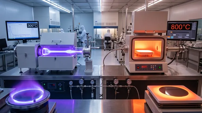
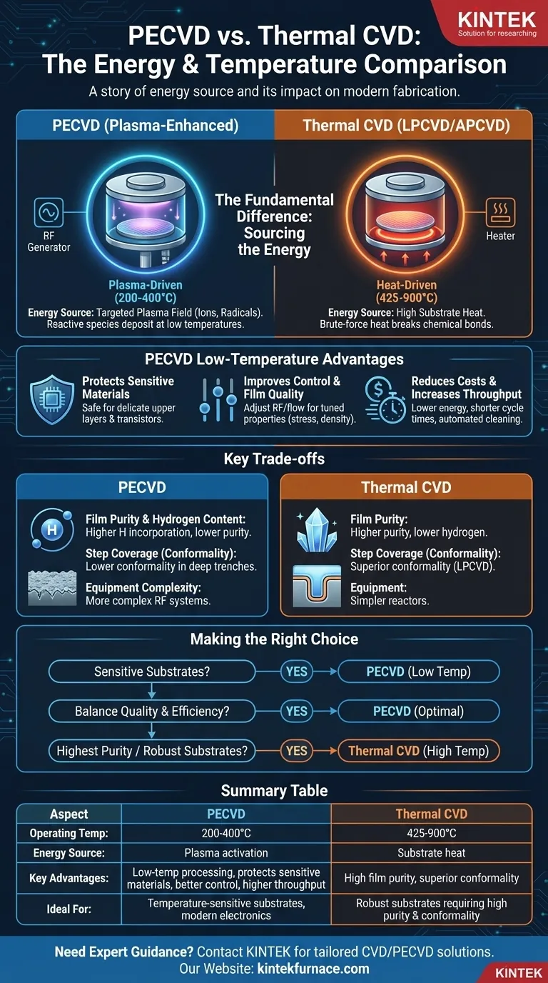
At its core, the comparison between Plasma-Enhanced Chemical Vapor Deposition (PECVD) and thermally driven processes like APCVD and LPCVD is a story of energy. PECVD uses plasma to energize reactant gases, allowing for high-quality film deposition at low temperatures (200-400°C). In contrast, thermal CVD methods rely exclusively on high substrate heat (425-900°C) to drive the chemical reaction, limiting their use with temperature-sensitive materials.
The fundamental difference is not merely the operating temperature, but the source of activation energy. Thermal CVD uses brute-force heat, while PECVD uses a targeted plasma field. This makes PECVD the default choice for modern semiconductor fabrication where protecting underlying device layers is paramount.
The Fundamental Difference: Sourcing the Energy
To choose the right process, you must first understand how each method initiates the chemical reaction needed to deposit a film.
Thermal CVD (LPCVD/APCVD): Driven by Heat
In a thermal CVD process, precursor gases are introduced into a heated chamber. The substrate itself is heated to a very high temperature.
This thermal energy serves one purpose: to be high enough to break the chemical bonds of the precursor gases and provide the energy for them to react and deposit on the substrate surface. The entire process is dictated by the temperature of the substrate.
PECVD: Driven by Plasma
PECVD fundamentally changes this dynamic by introducing a new energy source: plasma. An electric field (typically Radio Frequency, or RF) is used to excite the precursor gases into a plasma state.
This plasma is a highly energetic mixture of ions, electrons, and neutral radical species. These radicals are extremely reactive and readily deposit on the substrate, even if the substrate itself is at a much lower temperature. The plasma, not the substrate's heat, provides the primary energy for the reaction.
Key Implications of the Low-Temperature Advantage
Decoupling the reaction energy from the substrate temperature gives PECVD several critical advantages in a production environment.
Protecting Temperature-Sensitive Materials
This is the most significant benefit of PECVD. Modern integrated circuits are built in layers. By the time you are depositing upper layers, the delicate transistors and components already fabricated underneath cannot withstand the high temperatures of LPCVD without being damaged or having their electrical properties altered.
PECVD’s low-temperature process (200-400°C) allows for the deposition of high-quality dielectric films (like silicon nitride or silicon dioxide) on top of fully or partially fabricated devices without harming them.
Improving Control and Film Quality
Because PECVD uses plasma, operators gain additional variables to control the film's properties, such as stress, density, and composition. This is done by adjusting RF power, pressure, and gas flow rates.
This level of control allows for the engineering of films for specific applications, often resulting in layers with a lower likelihood of cracking and better overall quality than what could be achieved at a similar low temperature.
Reducing Costs and Increasing Throughput
The lower operating temperature directly translates to reduced energy consumption, lowering production costs.
Furthermore, because the system does not need to be ramped up to extreme temperatures and then cooled down, the cycle time per wafer can be shorter, contributing to higher overall throughput. Many PECVD systems also feature automated and easier chamber cleaning processes.
Understanding the Trade-offs
While PECVD is dominant in many areas, it is not a universal replacement for thermal CVD. An objective analysis requires acknowledging its limitations.
Film Purity and Hydrogen Content
PECVD films, particularly silicon nitride and silicon dioxide, often have a significant amount of hydrogen incorporated into them from the precursor gases (like silane, SiH₄). This hydrogen can affect the film's electrical properties and long-term stability.
High-temperature thermal CVD processes typically produce films with higher purity and lower hydrogen content because the heat is sufficient to drive off more byproducts.
Step Coverage (Conformality)
For applications requiring a perfectly uniform coating over complex, high-aspect-ratio trenches and structures, high-temperature LPCVD often provides superior conformality.
The higher surface temperature in LPCVD gives the depositing atoms more energy to move around (surface mobility) and find the most stable positions, allowing them to coat vertical sidewalls more effectively than in a typical low-temperature PECVD process.
Equipment Complexity
PECVD systems are inherently more complex than thermal reactors. They require RF power generators, matching networks, and sophisticated chamber designs to generate and contain the plasma. This can lead to a higher initial capital investment and more complex maintenance.
Making the Right Choice for Your Application
Your decision should be guided by your primary constraint: the thermal budget of your substrate and the desired properties of your final film.
- If your primary focus is compatibility with modern electronics or temperature-sensitive substrates: PECVD is the definitive choice due to its low-temperature operation.
- If your primary focus is the highest possible film purity and conformality on a robust substrate that can withstand heat: High-temperature LPCVD remains a superior option for specific applications like gate dielectrics or trench fills.
- If your primary focus is balancing film quality with operational efficiency and cost: PECVD offers an unmatched combination of good deposition rates, high film quality, and lower energy costs for a vast range of applications.
By understanding the fundamental energy mechanism, you can confidently select the deposition method that best aligns with your material constraints and performance goals.
Summary Table:
| Aspect | PECVD | Thermal CVD (e.g., LPCVD, APCVD) |
|---|---|---|
| Operating Temperature | 200-400°C | 425-900°C |
| Energy Source | Plasma activation | Substrate heat |
| Key Advantages | Low-temperature processing, protects sensitive materials, better control, higher throughput | High film purity, superior conformality |
| Ideal For | Temperature-sensitive substrates, modern electronics | Robust substrates requiring high purity and conformality |
Need expert guidance on selecting the right CVD system for your lab? KINTEK leverages exceptional R&D and in-house manufacturing to provide advanced high-temperature furnace solutions, including CVD/PECVD Systems. Our deep customization capabilities ensure precise alignment with your unique experimental needs, whether you're working with semiconductors, materials research, or other applications. Contact us today to discuss how our tailored solutions can enhance your deposition processes and drive innovation!
Visual Guide
Related Products
- Slide PECVD Tube Furnace with Liquid Gasifier PECVD Machine
- RF PECVD System Radio Frequency Plasma Enhanced Chemical Vapor Deposition
- Inclined Rotary Plasma Enhanced Chemical Deposition PECVD Tube Furnace Machine
- Inclined Rotary Plasma Enhanced Chemical Deposition PECVD Tube Furnace Machine
- Multi Heating Zones CVD Tube Furnace Machine for Chemical Vapor Deposition Equipment
People Also Ask
- In which industries is the tube furnace commonly used? Essential for Materials Science, Energy, and More
- How does PECVD equipment contribute to TOPCon bottom cells? Mastering Hydrogenation for Maximum Solar Efficiency
- What are the typical conditions for plasma-enhanced CVD processes? Achieve Low-Temperature Thin Film Deposition
- What are the advantages of using a tube furnace CVD system for Cu(111)/graphene? Superior Scalability and Quality
- What is plasma in the context of PECVD? Unlock Low-Temperature Thin Film Deposition


