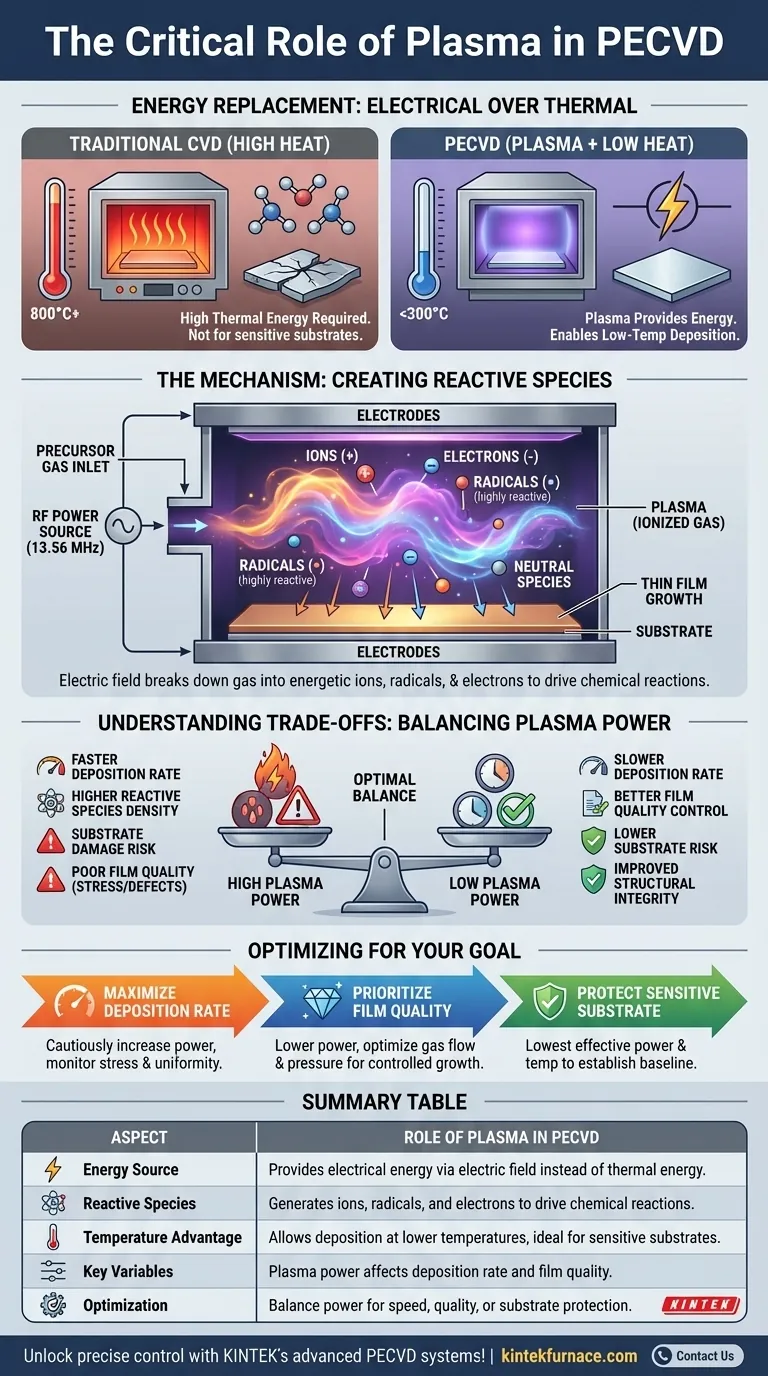
In Plasma-Enhanced Chemical Vapor Deposition (PECVD), plasma's primary role is to provide the energy needed to break down precursor gases into highly reactive chemical species. This is accomplished using an electric field rather than high heat. By creating ions, radicals, and electrons, the plasma activates the chemical reactions required for thin-film deposition at significantly lower temperatures than in traditional Chemical Vapor Deposition (CVD).
The central purpose of plasma in PECVD is to replace high thermal energy with electrical energy. This allows you to grow high-quality thin films on substrates that cannot withstand the high temperatures required by conventional deposition methods.
How Plasma Solves the Temperature Problem
The key advantage of PECVD lies in its ability to operate at low temperatures, and plasma is the mechanism that makes this possible.
The Limitation of Traditional CVD
Standard CVD processes rely exclusively on high thermal energy—often several hundred degrees Celsius—to break down stable gas molecules and initiate the chemical reactions needed for film growth. This heat requirement makes it unsuitable for temperature-sensitive substrates like plastics or certain electronic components.
Plasma as an Energy Substitute
PECVD circumvents this limitation by using plasma as an alternative energy source. Instead of heating the entire chamber, an electric field energizes the gas, transforming it into a plasma state.
Creating Reactive Chemical Species
This plasma is a partially ionized gas composed of a highly energetic mix of ions, free electrons, and electrically neutral but chemically aggressive radicals. These reactive species, not the inert precursor gas, are what drive the deposition process on the substrate surface.
The Mechanics of Plasma Generation
Creating and sustaining this plasma is a controlled process within the PECVD reactor.
The Role of the Electric Field
Plasma is typically generated by applying a high-frequency electric field between two parallel electrodes inside the vacuum chamber. The substrate is placed on one of these electrodes.
Common Energy Sources
The energy to create this field is most commonly supplied by a Radio Frequency (RF) source, often at a standardized industrial frequency of 13.56 MHz. However, Direct Current (DC) or other alternating current frequencies can also be used depending on the specific application and material being deposited.
Understanding the Trade-offs
While plasma is the key enabler for PECVD, its parameters must be carefully controlled to achieve the desired outcome. The primary variable is plasma power.
The Impact of Plasma Power
Increasing the plasma power generally increases the density of reactive species in the chamber. This can directly accelerate the film's deposition rate, which is often desirable for manufacturing efficiency.
The Risk of Excessive Power
However, higher power is not always better. Excessively energetic plasma can cause damage to the substrate through ion bombardment. It can also degrade the quality of the deposited film, leading to poor structural integrity, high internal stress, or undesirable chemical properties. A balance must be struck between deposition speed and film quality.
Optimizing Plasma for Your Deposition Goal
The ideal plasma conditions are entirely dependent on the specific film you are creating and the substrate you are using.
- If your primary focus is maximizing deposition rate: Cautiously increase plasma power while closely monitoring film stress and uniformity to find the optimal throughput without compromising the device.
- If your primary focus is film quality and integrity: Use lower plasma power settings and instead optimize other variables like gas flow rates and chamber pressure to achieve a controlled, high-quality growth environment.
- If your primary focus is protecting a sensitive substrate: Begin with the lowest effective plasma power and temperature to establish a baseline process, ensuring the substrate is not damaged during deposition.
Ultimately, mastering plasma gives you precise control over the energy within your deposition process, unlocking capabilities that heat alone cannot provide.
Summary Table:
| Aspect | Role of Plasma in PECVD |
|---|---|
| Energy Source | Provides electrical energy via electric field instead of thermal energy |
| Reactive Species | Generates ions, radicals, and electrons to drive chemical reactions |
| Temperature Advantage | Allows deposition at lower temperatures, ideal for sensitive substrates |
| Key Variables | Plasma power affects deposition rate and film quality |
| Optimization | Balance power for speed, quality, or substrate protection |
Unlock precise control for your thin-film deposition with KINTEK's advanced PECVD systems! Leveraging exceptional R&D and in-house manufacturing, we provide diverse laboratories with tailored high-temperature furnace solutions, including CVD/PECVD Systems. Our strong deep customization capability ensures we meet your unique experimental needs—whether you're working with sensitive substrates or aiming for high-quality film growth. Contact us today to discuss how our solutions can enhance your research and production efficiency!
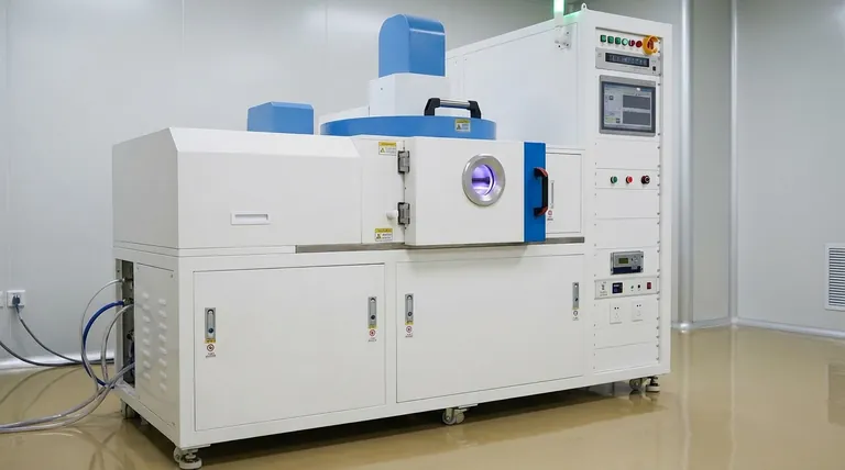
Visual Guide
Related Products
- RF PECVD System Radio Frequency Plasma Enhanced Chemical Vapor Deposition
- Slide PECVD Tube Furnace with Liquid Gasifier PECVD Machine
- Inclined Rotary Plasma Enhanced Chemical Deposition PECVD Tube Furnace Machine
- Inclined Rotary Plasma Enhanced Chemical Deposition PECVD Tube Furnace Machine
- 915MHz MPCVD Diamond Machine Microwave Plasma Chemical Vapor Deposition System Reactor
People Also Ask
- What are the applications of plasma enhanced chemical vapor deposition? Key Uses in Electronics, Optics & Materials
- What are some promising applications of PECVD-prepared 2D materials? Unlock Advanced Sensing and Optoelectronics
- How is silicon dioxide deposited from tetraethylorthosilicate (TEOS) in PECVD? Achieve Low-Temperature, High-Quality SiO2 Films
- What is PECVD specification? A Guide to Choosing the Right System for Your Lab
- How are deposition rates and film properties controlled in PECVD? Master Key Parameters for Optimal Thin Films


