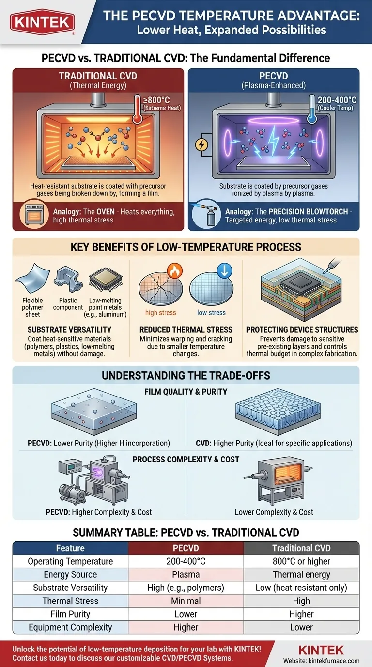
The primary advantage of PECVD is its dramatically lower operating temperature compared to traditional Chemical Vapor Deposition (CVD). While traditional CVD requires extreme heat (often 800°C or higher) to initiate chemical reactions, Plasma-Enhanced CVD (PECVD) operates at much cooler temperatures, typically in the 200-400°C range. This is made possible by using plasma, instead of just thermal energy, to break down the precursor gases and drive the deposition process.
The core difference is how energy is delivered to the system. Traditional CVD uses brute-force thermal energy, forcing a high-temperature environment. PECVD uses plasma to supply targeted energy for the chemical reaction, decoupling the reaction from the substrate temperature and enabling high-quality film growth on heat-sensitive materials.
The Fundamental Difference: Thermal vs. Plasma Energy
To understand the temperature advantage, you must first understand how each process supplies the energy needed to form a thin film from a gas.
How Traditional CVD Works
Traditional CVD relies exclusively on thermal energy. Precursor gases are introduced into a chamber containing a heated substrate. The high temperature provides the activation energy needed to break the chemical bonds in the gas molecules, allowing them to react and deposit as a solid film on the hot surface.
The process temperature is dictated entirely by the energy required for this chemical reaction.
How PECVD Works
PECVD introduces an additional energy source: plasma. An electric field is applied to the precursor gas, stripping electrons from atoms and creating a highly reactive, ionized gas—the plasma.
The energetic electrons and ions within the plasma collide with the gas molecules. These collisions, not high heat, provide the energy to break the chemical bonds. This allows the deposition reaction to occur at a significantly lower substrate temperature.
An Analogy: The Chef's Tools
Think of traditional CVD as an oven. To cook a specific part of a dish, you must heat the entire oven to a very high temperature, exposing everything inside to that heat.
PECVD is like using a precision blowtorch. The chef can apply intense, localized energy exactly where it's needed to trigger a reaction (like caramelizing sugar) without overheating the rest of the dish. The plasma is the blowtorch, providing targeted energy independent of the overall chamber temperature.
Key Benefits of a Low-Temperature Process
The ability to operate at lower temperatures is not just a minor improvement; it fundamentally expands the applications of thin film deposition.
Substrate Versatility
This is the most significant advantage. Materials that would melt, deform, or degrade in a traditional CVD furnace can be coated using PECVD. This includes polymers, plastics, and other organic materials.
It also enables deposition on fully or partially fabricated semiconductor wafers that contain metallic structures (like aluminum interconnects) with low melting points.
Reduced Thermal Stress
Heating and cooling a substrate, especially over a large temperature range, induces mechanical stress as the material expands and contracts. This can cause wafers to bow or even crack.
The smaller temperature delta in a PECVD process minimizes this thermal stress, improving the mechanical integrity of the substrate and the deposited film.
Protecting Existing Device Structures
In modern microfabrication, wafers undergo many process steps. A low-temperature PECVD step prevents unwanted diffusion of dopants or damage to sensitive, pre-existing layers on the device. This control over the "thermal budget" is critical for manufacturing complex integrated circuits.
Understanding the Trade-offs
While powerful, the low-temperature advantage of PECVD comes with considerations that may make traditional CVD preferable in certain scenarios.
Film Quality and Purity
Because the deposition mechanism is different, the resulting film is not identical. PECVD films often have a higher concentration of incorporated hydrogen, as the precursor gases are not as completely dissociated.
For applications demanding the highest possible film purity, density, or crystallinity (like certain gate oxides), the high-temperature environment of traditional CVD can produce a superior result, assuming the substrate can tolerate the heat.
Process Complexity and Cost
A PECVD system is inherently more complex than a traditional thermal CVD reactor. It requires RF power generators, impedance matching networks, and advanced vacuum systems to create and sustain the plasma. This translates to higher equipment cost and potentially more complex maintenance.
Making the Right Choice for Your Application
Your choice between PECVD and traditional CVD depends entirely on your substrate limitations and your desired film properties.
- If your primary focus is compatibility with heat-sensitive materials: PECVD is the definitive and often only choice for coating polymers, plastics, or devices with low-melting-point metals.
- If your primary focus is achieving the highest possible film purity and density: Traditional high-temperature CVD may be required, provided your substrate can withstand the intense heat.
- If your primary focus is managing the thermal budget in complex device fabrication: PECVD offers critical control to deposit films late in the manufacturing process without damaging previously fabricated layers.
By understanding the role of energy in each process, you can select the deposition method that best protects your substrate while achieving your desired film properties.
Summary Table:
| Feature | PECVD | Traditional CVD |
|---|---|---|
| Operating Temperature | 200-400°C | 800°C or higher |
| Energy Source | Plasma | Thermal energy |
| Substrate Versatility | High (e.g., polymers, low-melting-point metals) | Low (heat-resistant materials only) |
| Thermal Stress | Minimal | High |
| Film Purity | Lower (may have hydrogen incorporation) | Higher |
| Equipment Complexity | Higher | Lower |
Unlock the potential of low-temperature deposition for your lab with KINTEK! Leveraging exceptional R&D and in-house manufacturing, we provide advanced high-temperature furnace solutions, including CVD/PECVD Systems, tailored to your unique experimental needs. Our deep customization capability ensures precise performance for heat-sensitive materials. Contact us today to discuss how our PECVD systems can enhance your research and production efficiency!
Visual Guide
Related Products
- Slide PECVD Tube Furnace with Liquid Gasifier PECVD Machine
- RF PECVD System Radio Frequency Plasma Enhanced Chemical Vapor Deposition
- Inclined Rotary Plasma Enhanced Chemical Deposition PECVD Tube Furnace Machine
- Inclined Rotary Plasma Enhanced Chemical Deposition PECVD Tube Furnace Machine
- Multi Heating Zones CVD Tube Furnace Machine for Chemical Vapor Deposition Equipment
People Also Ask
- What role does a Tube Furnace play in the CVD growth of carbon nanotubes? Achieve High-Purity CNT Synthesis
- In which industries is the tube furnace commonly used? Essential for Materials Science, Energy, and More
- What is plasma in the context of PECVD? Unlock Low-Temperature Thin Film Deposition
- What are the main advantages of PECVD tube furnaces compared to CVD tube furnaces? Lower Temp, Faster Deposition, and More
- What are the typical conditions for plasma-enhanced CVD processes? Achieve Low-Temperature Thin Film Deposition


