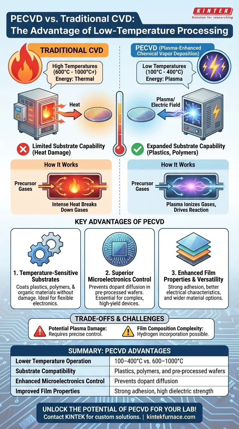
The defining advantage of PECVD is its ability to deposit high-quality thin films at significantly lower temperatures than traditional Chemical Vapor Deposition (CVD) methods. This is achieved by using plasma to energize the precursor gases, replacing the high thermal energy required in conventional processes. This fundamental difference unlocks capabilities that are critical for modern manufacturing, especially in electronics and materials science.
PECVD overcomes the primary limitation of traditional CVD—high heat. By using plasma instead of thermal energy to drive chemical reactions, it allows for the coating of temperature-sensitive materials that would otherwise be damaged or destroyed, dramatically expanding the scope of what can be manufactured.
The Fundamental Difference: Plasma vs. Thermal Energy
To understand the advantages of Plasma-Enhanced Chemical Vapor Deposition (PECVD), we must first distinguish how it works compared to its traditional thermal counterpart. The core difference lies in the source of energy used to initiate the film-forming reaction.
How Traditional CVD Works
Traditional thermal CVD relies purely on high temperatures, often ranging from 600°C to over 1000°C, to provide the necessary activation energy.
Precursor gases are introduced into a hot-wall reactor, where the intense heat breaks them down. The resulting reactive species then deposit onto the substrate to form the desired thin film.
How PECVD Changes the Game
PECVD operates at much lower temperatures, typically between 100°C and 400°C. Instead of heat, it uses an electric field to ionize the precursor gases, creating a plasma.
This plasma is a highly energetic state of matter containing a dense mixture of ions, electrons, and reactive free radicals. These species are chemically reactive enough to form a high-quality film upon contacting the substrate, without requiring a high thermal budget.
Key Advantages of Low-Temperature Processing
The ability to operate at low temperatures is not just an incremental improvement; it is a transformative capability that yields several critical advantages.
Compatibility with Temperature-Sensitive Substrates
This is the most direct and impactful benefit. Many advanced materials cannot withstand the high temperatures of traditional CVD.
PECVD makes it possible to deposit films on substrates like plastics, polymers, and organic materials. This capability is essential for applications like flexible electronics, protective coatings on consumer goods, and biomedical devices.
Superior Control in Microelectronics
In semiconductor manufacturing, wafers already contain intricate, multi-layered circuits. Exposing them to high temperatures can cause previously implanted dopants to diffuse, or move from their intended positions.
This diffusion blurs the boundaries of nanoscale components, degrading device performance and yield. PECVD's low thermal budget prevents this unwanted dopant movement, making it indispensable for fabricating the smaller, faster, and more complex integrated circuits in modern electronics.
Enhanced Film Properties and Versatility
The plasma environment allows for the deposition of a wider range of materials compared to many thermal CVD processes.
Furthermore, the films often exhibit excellent properties, such as strong substrate adhesion and good electrical characteristics (e.g., high dielectric strength). The lower thermal stress during deposition contributes to more stable and durable films.
Understanding the Trade-offs
While powerful, PECVD is not a universal solution. An objective assessment requires acknowledging its specific challenges.
Potential for Plasma-Induced Damage
The high-energy ions within the plasma, while useful for driving reactions, can also physically bombard the substrate and the growing film. If not precisely controlled, this can introduce defects or surface damage, impacting the material's performance.
Film Composition Complexity
PECVD processes often use precursor gases containing hydrogen (e.g., silane, SiH₄). It is common for some hydrogen to be incorporated into the final film, which can alter its optical, electrical, and mechanical properties. Managing this requires careful process tuning.
Equipment and Process Complexity
A PECVD system is inherently more complex than a basic thermal CVD reactor. It requires additional components like RF or microwave power generators, impedance matching networks, and sophisticated vacuum systems, which can lead to higher capital costs and a more intricate process to control.
Making the Right Choice for Your Goal
Selecting the correct deposition method requires matching the technology's strengths to your specific application and constraints.
- If your primary focus is coating heat-sensitive materials: PECVD is the definitive choice due to its low-temperature operation, enabling work with plastics, polymers, or pre-processed wafers.
- If your primary focus is fabricating advanced semiconductors: PECVD provides the essential low thermal budget to prevent dopant diffusion and maintain the integrity of nanoscale devices.
- If your primary focus is depositing simple, robust films on heat-tolerant substrates: Traditional thermal CVD can be a more straightforward and cost-effective method if the material can withstand the heat.
By understanding the core trade-off between thermal and plasma energy, you can confidently select the deposition technology that aligns with your material constraints and performance goals.
Summary Table:
| Advantage | Description |
|---|---|
| Lower Temperature Operation | Deposits films at 100–400°C vs. 600–1000°C in CVD, enabling use with heat-sensitive materials. |
| Substrate Compatibility | Allows coating of plastics, polymers, and pre-processed wafers without damage. |
| Enhanced Microelectronics Control | Prevents dopant diffusion in semiconductors, maintaining device integrity and performance. |
| Improved Film Properties | Offers strong adhesion, high dielectric strength, and versatility in material deposition. |
Unlock the potential of PECVD for your lab! Leveraging exceptional R&D and in-house manufacturing, KINTEK provides diverse laboratories with advanced high-temperature furnace solutions, including CVD/PECVD Systems. Our strong deep customization capability ensures we precisely meet your unique experimental requirements. Contact us today to discuss how our tailored PECVD solutions can enhance your thin film deposition processes and drive innovation in your projects!
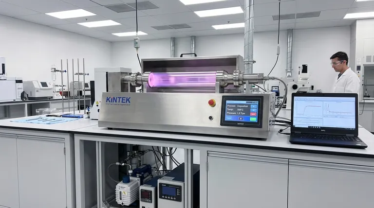
Visual Guide
Related Products
- Slide PECVD Tube Furnace with Liquid Gasifier PECVD Machine
- RF PECVD System Radio Frequency Plasma Enhanced Chemical Vapor Deposition
- Inclined Rotary Plasma Enhanced Chemical Deposition PECVD Tube Furnace Machine
- Inclined Rotary Plasma Enhanced Chemical Deposition PECVD Tube Furnace Machine
- Multi Heating Zones CVD Tube Furnace Machine for Chemical Vapor Deposition Equipment
People Also Ask
- What are the disadvantages of tube furnace cracking when processing heavy raw materials? Avoid Costly Downtime and Inefficiency
- What are the typical conditions for plasma-enhanced CVD processes? Achieve Low-Temperature Thin Film Deposition
- In which industries is the tube furnace commonly used? Essential for Materials Science, Energy, and More
- What is plasma in the context of PECVD? Unlock Low-Temperature Thin Film Deposition
- What plasma source is used in PE-CVD tube furnaces? Unlock Low-Temperature, High-Quality Deposition


