Beyond standard insulation, Plasma-Enhanced Chemical Vapor Deposition (PECVD) is a cornerstone technology for creating a new class of advanced materials. Its applications range from depositing high-quality diamond and Diamond-Like Carbon (DLC) films for wear-resistant and optical components to creating specialized biocompatible polymer coatings for medical implants and unique low-k dielectrics essential for next-generation microchips.
The true power of PECVD lies not just in the materials it can deposit, but in its ability to do so at low temperatures. This single characteristic unlocks the use of temperature-sensitive substrates, enabling advanced material applications that are simply not feasible with conventional high-heat deposition methods.
The Core Advantage: Low Temperature, High Energy
The fundamental difference between PECVD and traditional Chemical Vapor Deposition (CVD) is how it supplies the energy needed for the chemical reaction. This distinction is the source of all its advanced capabilities.
Dissociating Molecules Without Extreme Heat
Traditional CVD requires very high temperatures (often >600°C) to break down precursor gas molecules and deposit a film. In PECVD, this energy is supplied by an electromagnetic field that generates plasma. The plasma creates highly reactive ions and free radicals that can form a high-quality film at much lower temperatures, typically between 200-400°C.
Enabling Temperature-Sensitive Substrates
This low-temperature process means PECVD can coat materials that would be damaged or destroyed by the heat of traditional CVD. This includes polymers, plastics, and fully fabricated microelectronic devices that already contain sensitive metallic layers.
Advanced Material Deposition in Microelectronics
While PECVD is standard for basic insulation, its true value is in enabling the performance of modern, high-density integrated circuits.
Foundational Dielectrics (SiO₂, Si₃N₄)
Depositing silicon dioxide and silicon nitride films is a primary use of PECVD. These films serve as crucial inter-metal dielectrics for insulation, as passivation layers to protect the chip from moisture and contamination, and for creating capacitor structures.
High-Performance Low-k Dielectrics
As transistors shrink, the delay caused by capacitance between wires becomes a major bottleneck. PECVD can deposit advanced low-k dielectrics, such as carbon-doped silicon oxides (SiCOH) or fluorine-doped silicate glass (SiOF), which reduce this parasitic capacitance and allow for faster chip performance.
Amorphous Silicon for Solar and Displays
PECVD is essential for depositing layers of amorphous silicon (a-Si). This material is the backbone of thin-film solar cells and the thin-film transistors (TFTs) that control the pixels in modern flat-panel displays.
Beyond Silicon: Pushing Material Boundaries
PECVD's versatility extends far beyond conventional semiconductor materials, enabling innovation in mechanical, optical, and biomedical fields.
Diamond and Diamond-Like Carbon (DLC)
By using hydrocarbon gases, PECVD can create films of Diamond-Like Carbon (DLC). These films are extremely hard, have a low coefficient of friction, and are chemically inert, making them ideal for wear-resistant coatings on tools, automotive parts, and optical components. It can even be used to grow high-quality synthetic diamond films.
Biocompatible and Polymeric Coatings
PECVD can deposit thin, stable, and pinhole-free polymer films. This capability is used to create biocompatible coatings on medical implants to improve their integration with the body or to form barrier layers in advanced food packaging.
Corrosion and Chemical Resistant Layers
The process can deposit unique compounds and nitrides that offer exceptional resistance to corrosion and chemical attack. These protective coatings are applied in harsh industrial environments to extend the life of critical components.
Understanding the Trade-offs
No technology is a universal solution. Understanding the limitations of PECVD is critical for making an informed decision.
Film Purity and Density
Because the deposition occurs at lower temperatures, PECVD films can sometimes have lower density and incorporate more impurities (such as hydrogen from precursor gases) compared to films from high-temperature CVD. For applications demanding the absolute highest purity and crystalline perfection, thermal CVD may be superior if the substrate can tolerate the heat.
Plasma-Induced Damage
The high-energy plasma, while beneficial for the reaction, can sometimes cause physical or electrical damage to the surface of the substrate. This is a critical consideration in microelectronics, where device performance is highly sensitive to surface defects.
Process Complexity
The chemistry within a plasma is extremely complex and can be difficult to control and reproduce perfectly. Maintaining process stability to achieve consistent film properties across a large substrate or from run to run requires sophisticated equipment and control.
Making the Right Choice for Your Application
Selecting the right deposition technology depends entirely on your end goal and material constraints.
- If your primary focus is ultimate chip speed: Leverage PECVD for depositing advanced low-k dielectrics to minimize signal delay in high-performance integrated circuits.
- If your primary focus is mechanical durability or biocompatibility: Use PECVD to apply Diamond-Like Carbon (DLC) or specialized polymer coatings that cannot be deposited with high-heat methods.
- If your primary focus is coating a temperature-sensitive material: PECVD is often the only viable choice for depositing high-quality ceramic or silicon-based films onto plastics, polymers, or finished devices.
Ultimately, PECVD serves as a powerful tool that decouples the deposition reaction from thermal budget, unlocking material combinations and innovations that drive technology forward.
Summary Table:
| Application Area | Key Materials Deposited | Primary Benefits |
|---|---|---|
| Microelectronics | Low-k dielectrics (e.g., SiCOH), Amorphous Silicon | Faster chip performance, Enables thin-film transistors |
| Mechanical/Optical | Diamond-Like Carbon (DLC), Diamond Films | High hardness, Wear resistance, Low friction |
| Biomedical | Biocompatible Polymer Coatings | Improved implant integration, Barrier properties |
| General Industrial | Corrosion-Resistant Layers | Extended component life in harsh environments |
Ready to elevate your lab's capabilities with advanced PECVD solutions? At KINTEK, we leverage exceptional R&D and in-house manufacturing to provide diverse laboratories with cutting-edge high-temperature furnace systems, including CVD/PECVD systems. Our strong deep customization capability ensures we precisely meet your unique experimental needs, whether for microelectronics, biomedical coatings, or durable material applications. Contact us today to discuss how our tailored solutions can drive your innovations forward!
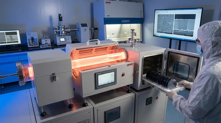
Visual Guide

Related Products
- RF PECVD System Radio Frequency Plasma Enhanced Chemical Vapor Deposition
- Slide PECVD Tube Furnace with Liquid Gasifier PECVD Machine
- Inclined Rotary Plasma Enhanced Chemical Deposition PECVD Tube Furnace Machine
- Inclined Rotary Plasma Enhanced Chemical Deposition PECVD Tube Furnace Machine
- Cylindrical Resonator MPCVD Machine System for Lab Diamond Growth
People Also Ask
- What is the role of RF power in PECVD and how does the RF-PECVD process work? Master Thin Film Deposition Control
- How does film quality compare between PECVD and CVD? Choose the Best Method for Your Substrate
- What are the key advantages of PECVD technology? Achieve Low-Temperature, High-Quality Thin Film Deposition
- What are the applications of plasma enhanced chemical vapor deposition? Key Uses in Electronics, Optics & Materials
- What are some promising applications of PECVD-prepared 2D materials? Unlock Advanced Sensing and Optoelectronics


