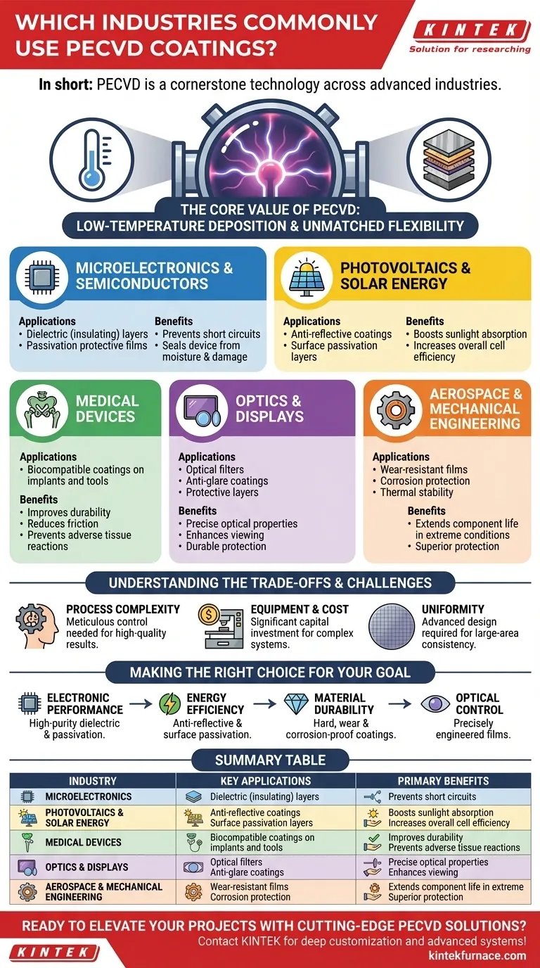
In short, Plasma-Enhanced Chemical Vapor Deposition (PECVD) is a cornerstone technology used across a wide range of advanced industries. Its most significant applications are found in microelectronics for creating semiconductor devices, in the manufacturing of high-efficiency solar cells, and in the medical field for producing biocompatible coatings on implants and tools.
The core value of PECVD is its ability to deposit high-performance, functional thin films at low temperatures. This single advantage unlocks its use on heat-sensitive materials and complex components that would be damaged by traditional high-temperature deposition methods.
The Foundation: Why is PECVD So Versatile?
The widespread adoption of PECVD stems from its unique low-temperature process, which offers exceptional control and material flexibility.
A Low-Temperature Advantage
Unlike traditional Chemical Vapor Deposition (CVD), which requires very high temperatures to initiate chemical reactions, PECVD uses an energy-rich plasma.
This plasma provides the energy needed to break down precursor gases and deposit a thin film onto a surface. By operating at significantly lower temperatures, PECVD can coat sensitive electronics, plastics, and other materials without causing thermal damage.
Unmatched Material Flexibility
The PECVD process is not limited to a single type of material. It can be used to deposit a diverse range of functional coatings.
This includes insulating oxides, conductive nitrides, and even specialized polymers like silicones and fluorocarbons. This adaptability allows engineers to select the perfect material for a specific performance goal.
Key Industrial Applications of PECVD
This versatility has made PECVD an essential process in nearly every high-tech industry. It is not just one tool, but a platform for enabling countless modern innovations.
Microelectronics and Semiconductors
This is arguably the largest and most critical application of PECVD. It is used to deposit dielectric (insulating) layers between conductive paths on a microchip, preventing short circuits.
It is also used for passivation layers, which are thin, protective films that seal the final semiconductor device from moisture, contamination, and mechanical damage.
Photovoltaics and Solar Energy
Efficiency is the ultimate goal in solar cell production. PECVD plays two crucial roles here.
First, it is used to apply anti-reflective coatings to the surface of the solar cell, ensuring that a maximum amount of sunlight is absorbed rather than reflected away. Second, it creates surface passivation layers that reduce energy losses within the silicon wafer, directly boosting the cell's overall efficiency.
Optics and Displays
PECVD allows for the precise engineering of a film's optical properties, such as its refractive index.
This capability is used to create sophisticated optical filters, high-performance anti-glare coatings for flat-panel displays, and durable protective coatings for lenses and sunglasses.
Medical Devices
When a device is implanted in the human body, its surface interaction is critical. PECVD is used to apply ultra-thin, biocompatible coatings to medical implants and surgical tools.
These coatings can improve durability, reduce friction, and prevent adverse reactions with body tissue, enhancing both the safety and longevity of the device.
Aerospace and Mechanical Engineering
Components in aerospace and heavy industry operate in extreme conditions. PECVD provides a solution by depositing highly durable films.
These coatings offer superior wear resistance, corrosion protection, and thermal stability, extending the operational life of critical parts in engines and structural components.
Understanding the Trade-offs and Challenges
While incredibly powerful, PECVD is a sophisticated process that requires significant expertise and investment to master.
Process Complexity
The quality of a PECVD film is determined by a complex interplay of variables, including gas composition, pressure, temperature, and plasma power. Achieving a consistent, high-quality result requires meticulous control and process optimization.
Equipment and Cost
PECVD systems are complex vacuum deposition tools that represent a significant capital investment. The cost and infrastructure required mean it is best suited for high-value manufacturing where performance justifies the expense.
Uniformity over Large Areas
Depositing a perfectly uniform film across a large surface (like a large-area display or a wide silicon wafer) can be challenging. Advanced system design is required to manage plasma distribution and ensure consistent film thickness and properties.
Making the Right Choice for Your Goal
PECVD is not a single solution but a platform technology. The way you apply it depends entirely on the problem you are trying to solve.
- If your primary focus is electronic performance and miniaturization: Use PECVD to deposit the high-purity dielectric and passivation layers essential for modern integrated circuits.
- If your primary focus is energy efficiency: Leverage PECVD to create the anti-reflective and surface passivation coatings that directly boost the output of photovoltaic cells.
- If your primary focus is material durability: Apply PECVD for creating hard, wear-resistant, or corrosion-proof coatings on mechanical, aerospace, or medical components.
- If your primary focus is optical control: Utilize PECVD to precisely engineer the refractive index of films for advanced filters, lenses, and displays.
Ultimately, PECVD's ability to create functional surfaces is a key enabler for much of the technology that defines our world.
Summary Table:
| Industry | Key PECVD Applications | Primary Benefits |
|---|---|---|
| Microelectronics | Dielectric layers, passivation films | Prevents short circuits, protects from moisture and contamination |
| Photovoltaics | Anti-reflective coatings, surface passivation | Increases solar cell efficiency by reducing reflection and energy loss |
| Medical Devices | Biocompatible coatings on implants and tools | Improves durability, reduces friction, prevents adverse tissue reactions |
| Optics and Displays | Optical filters, anti-glare coatings | Enhances optical properties, provides durable protection for lenses and screens |
| Aerospace and Mechanical | Wear-resistant, corrosion-protective films | Extends component life in extreme conditions, offers thermal stability |
Ready to elevate your projects with cutting-edge PECVD solutions? At KINTEK, we leverage exceptional R&D and in-house manufacturing to provide advanced high-temperature furnace systems, including our specialized CVD/PECVD Systems. Our strong deep customization capability ensures we can precisely meet your unique experimental and production needs, whether you're in microelectronics, solar energy, medical devices, optics, or aerospace. Contact us today to discuss how our tailored PECVD technologies can drive innovation and efficiency in your industry!
Visual Guide
Related Products
- RF PECVD System Radio Frequency Plasma Enhanced Chemical Vapor Deposition
- Inclined Rotary Plasma Enhanced Chemical Deposition PECVD Tube Furnace Machine
- Slide PECVD Tube Furnace with Liquid Gasifier PECVD Machine
- HFCVD Machine System Equipment for Drawing Die Nano Diamond Coating
- Inclined Rotary Plasma Enhanced Chemical Deposition PECVD Tube Furnace Machine
People Also Ask
- What are some promising applications of PECVD-prepared 2D materials? Unlock Advanced Sensing and Optoelectronics
- What is the role of RF power in PECVD and how does the RF-PECVD process work? Master Thin Film Deposition Control
- What are the applications of plasma enhanced chemical vapor deposition? Key Uses in Electronics, Optics & Materials
- How are deposition rates and film properties controlled in PECVD? Master Key Parameters for Optimal Thin Films
- How is silicon dioxide deposited from tetraethylorthosilicate (TEOS) in PECVD? Achieve Low-Temperature, High-Quality SiO2 Films


