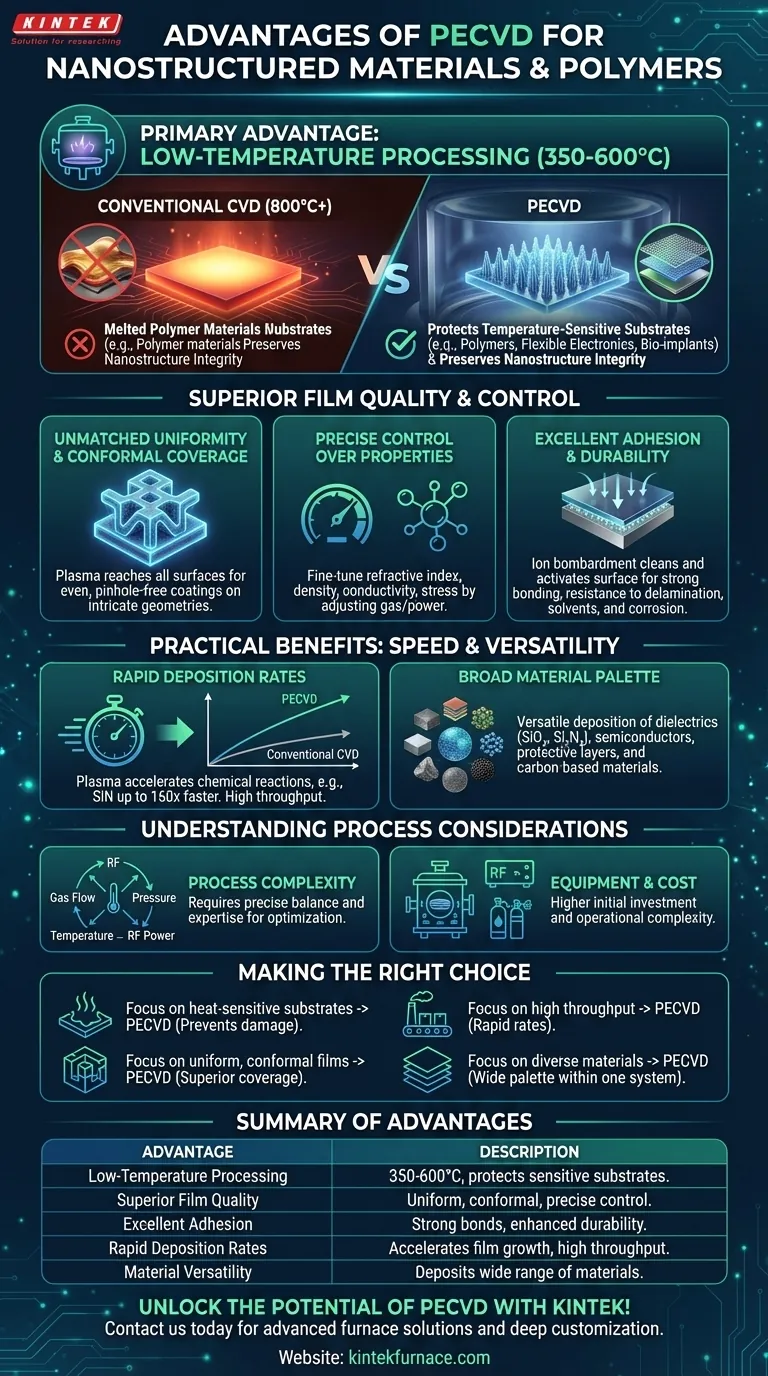
At its core, the primary advantage of Plasma-Enhanced Chemical Vapor Deposition (PECVD) for nanostructured materials and polymers is its ability to deposit high-quality films at significantly lower temperatures than conventional methods. This low-temperature operation is critical for preventing thermal damage to sensitive materials while enabling precise control over film thickness, composition, and uniformity, making it an indispensable tool for advanced material fabrication.
PECVD overcomes the fundamental limitation of traditional high-temperature deposition. It uses an energy-rich plasma to drive chemical reactions, allowing you to create durable, uniform, and functional thin films on materials—like polymers and complex nanostructures—that would otherwise be damaged or destroyed by heat.
The Fundamental Advantage: Low-Temperature Processing
The single most important benefit of PECVD is its low operating temperature, typically between 350-600°C, and often much lower for specific applications. This is a dramatic reduction compared to conventional Chemical Vapor Deposition (CVD), which can require temperatures exceeding 800°C.
Protecting Temperature-Sensitive Substrates
Polymers and other organic materials have low melting or glass transition temperatures. High-temperature processes would cause them to warp, melt, or decompose entirely.
PECVD’s low-temperature environment is the key enabling factor for depositing functional coatings directly onto polymer-based devices, flexible electronics, and medical implants without damaging the underlying substrate.
Preserving Nanostructure Integrity
Many nanostructured materials derive their unique properties from their precise size, shape, and arrangement.
Exposing these delicate architectures to high heat can cause them to reflow, agglomerate, or lose their intended structure. PECVD preserves the integrity of these pre-fabricated features during the coating process.
Achieving Superior Film Quality and Control
Beyond temperature, PECVD offers a level of control that is essential for the demanding requirements of nanotechnology. The plasma environment provides unique levers for tuning the final film properties.
Unmatched Uniformity and Conformal Coverage
The energized gas species in the plasma can reach and react on all exposed surfaces of a complex, three-dimensional object.
This results in a highly uniform and conformal coating that covers intricate nanostructures evenly, a feat that is difficult for line-of-sight deposition methods. This process also produces films with fewer pinholes and a lower likelihood of cracking.
Precise Control Over Film Properties
By adjusting parameters like gas composition, pressure, and plasma power, you can precisely tune the deposited film’s properties.
This allows for the creation of materials with specific refractive indices, densities, electrical conductivities, and internal stress levels. This control is vital for fabricating functional nanodevices and specialized polymer surfaces.
Excellent Adhesion and Durability
The ion bombardment inherent in the plasma process can gently clean and activate the substrate surface just before deposition.
This leads to excellent adhesion between the film and the substrate. The resulting low-stress films are more durable and less prone to delamination or cracking, providing high solvent and corrosion resistance.
The Practical Benefits: Speed and Versatility
For both research and industrial applications, efficiency and flexibility are critical. PECVD excels in both areas compared to many alternative thin-film techniques.
Rapid Deposition Rates
The plasma significantly accelerates the chemical reactions required for film growth.
Deposition rates can be orders of magnitude faster than conventional CVD. For example, silicon nitride deposition via PECVD can be up to 160 times faster, enabling higher throughput for manufacturing.
A Broad Material Palette
PECVD is not limited to a single class of materials. It is a highly versatile technique capable of depositing a wide range of substances.
This includes crucial materials for nanoelectronics and functional surfaces like dielectrics (SiO₂, Si₃N₄), semiconductors (silicon), protective layers (metal oxides, nitrides), and various carbon-based materials.
Understanding the Practical Considerations
While powerful, PECVD is not without its complexities. Achieving its benefits requires a clear understanding of the process requirements.
Process Complexity
The quality of a PECVD film is highly dependent on a precise balance of multiple variables, including gas flow rates, pressure, temperature, and RF power.
Optimizing a process for a specific material and substrate requires significant expertise. The plasma chemistry itself can be complex, and improper parameters can lead to poor film quality or contamination.
Equipment and Cost
PECVD systems require sophisticated hardware, including vacuum chambers, high-purity gas delivery systems, and radio-frequency (RF) power generators to create the plasma.
This represents a higher initial capital investment and greater operational complexity compared to simpler, atmospheric-pressure deposition techniques.
Making the Right Choice for Your Goal
Deciding on a deposition technique depends entirely on your project's specific constraints and desired outcomes.
- If your primary focus is coating heat-sensitive substrates like polymers: PECVD is the ideal choice due to its fundamentally low-temperature operation, which prevents substrate damage.
- If your primary focus is creating highly uniform, conformal films on complex nanostructures: PECVD's plasma-driven process provides the superior coverage and film quality needed for intricate 3D geometries.
- If your primary focus is achieving high throughput in a production environment: PECVD's rapid deposition rates offer a significant efficiency advantage over slower, conventional deposition methods.
- If your primary focus is creating multi-layer devices with diverse materials: PECVD's versatility allows you to deposit a wide range of dielectrics, semiconductors, and protective layers within a single system.
Ultimately, PECVD empowers you to engineer advanced materials by uniquely combining low-temperature processing with high-quality results and practical speed.
Summary Table:
| Advantage | Description |
|---|---|
| Low-Temperature Processing | Operates at 350-600°C, preventing thermal damage to sensitive substrates like polymers and nanostructures. |
| Superior Film Quality | Ensures uniform, conformal coatings with precise control over thickness, composition, and properties. |
| Excellent Adhesion | Provides strong film-substrate bonds, reducing delamination and enhancing durability. |
| Rapid Deposition Rates | Accelerates film growth, offering high throughput compared to conventional methods. |
| Material Versatility | Deposits a wide range of materials, including dielectrics, semiconductors, and protective layers. |
Unlock the full potential of PECVD for your laboratory with KINTEK! Leveraging exceptional R&D and in-house manufacturing, we provide advanced high-temperature furnace solutions tailored to your needs. Our product line, including Muffle, Tube, Rotary Furnaces, Vacuum & Atmosphere Furnaces, and CVD/PECVD Systems, is complemented by strong deep customization capabilities to precisely meet unique experimental requirements. Whether you're working with nanostructured materials, polymers, or other sensitive substrates, our expertise ensures optimal performance and efficiency. Contact us today to discuss how we can enhance your material fabrication processes!
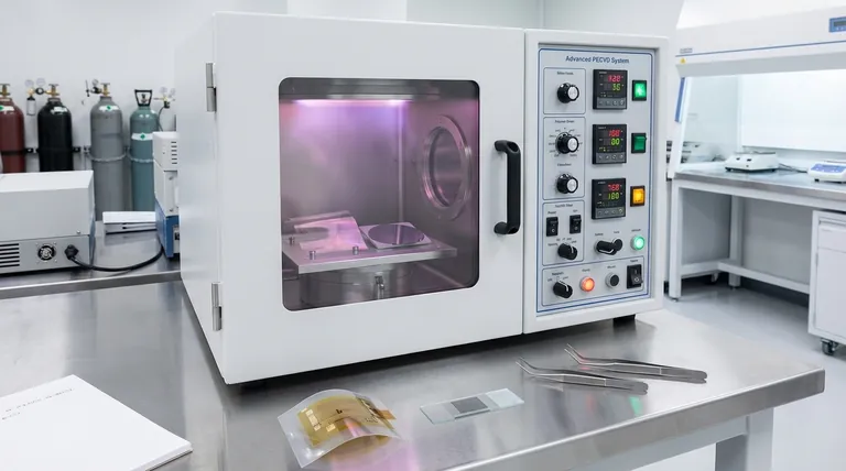
Visual Guide
Related Products
- Slide PECVD Tube Furnace with Liquid Gasifier PECVD Machine
- RF PECVD System Radio Frequency Plasma Enhanced Chemical Vapor Deposition
- Inclined Rotary Plasma Enhanced Chemical Deposition PECVD Tube Furnace Machine
- Inclined Rotary Plasma Enhanced Chemical Deposition PECVD Tube Furnace Machine
- Multi Heating Zones CVD Tube Furnace Machine for Chemical Vapor Deposition Equipment
People Also Ask
- How does PECVD equipment contribute to TOPCon bottom cells? Mastering Hydrogenation for Maximum Solar Efficiency
- In which industries is the tube furnace commonly used? Essential for Materials Science, Energy, and More
- What are the typical conditions for plasma-enhanced CVD processes? Achieve Low-Temperature Thin Film Deposition
- What is plasma in the context of PECVD? Unlock Low-Temperature Thin Film Deposition
- How does a hydrogen reduction environment in an industrial tube furnace facilitate gold-copper alloy microspheres?


