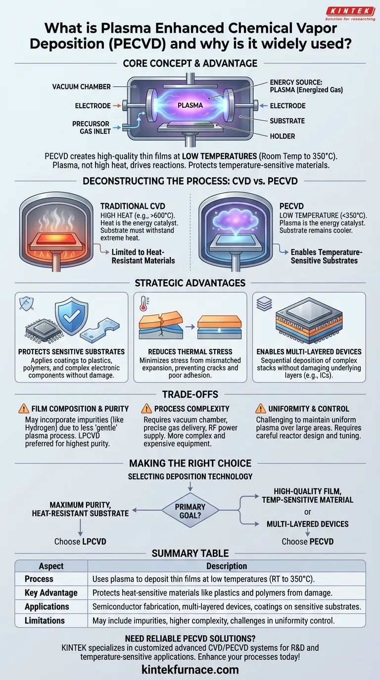
At its core, Plasma Enhanced Chemical Vapor Deposition (PECVD) is a process for creating high-quality, thin films on a surface. It stands out from other methods because it uses an energized gas, or plasma, to drive the chemical reactions needed for deposition. This fundamental difference allows PECVD to operate at much lower temperatures than traditional Chemical Vapor Deposition (CVD), making it exceptionally versatile and indispensable in modern manufacturing.
The central advantage of PECVD is that it decouples the reaction energy from the substrate's temperature. By using plasma to break down precursor gases instead of high heat, it enables the coating of temperature-sensitive materials that would otherwise be damaged or destroyed by conventional deposition processes.
Deconstructing the PECVD Process
To understand why PECVD is so widely used, we must first compare it to its predecessor, traditional Chemical Vapor Deposition (CVD). The key difference lies in how each process supplies the necessary energy.
The Problem with Traditional CVD
Standard CVD works like a high-temperature oven. It heats a substrate (the object to be coated) to very high temperatures, often over 600°C. Precursor gases are then introduced, and the intense heat breaks them down, causing them to react and deposit a solid film onto the hot substrate. This process is effective but has a significant limitation: it can only be used on materials that can withstand extreme heat.
The Role of Plasma
PECVD solves this problem by introducing a new energy source: plasma. Plasma is often called the fourth state of matter and is created by applying energy (typically a radio-frequency field) to a gas at low pressure. This process strips electrons from the gas molecules, creating a highly energized mixture of ions, electrons, and neutral particles.
Plasma as the Energy Catalyst
In a PECVD chamber, this plasma provides the energy needed to break apart the precursor gas molecules. The energetic collisions within the plasma are sufficient to initiate chemical reactions that lead to film deposition. Because the plasma—not heat—is doing the heavy lifting, the substrate itself can remain at a much lower temperature, typically between room temperature and 350°C.
The Strategic Advantage of Low-Temperature Processing
The ability to deposit films at low temperatures is not just a minor improvement; it is a transformative capability that unlocks new possibilities in materials science and device fabrication.
Protecting Sensitive Substrates
Many advanced materials and devices cannot tolerate the high temperatures of traditional CVD. This includes plastics, polymers, and complex electronic components that have already undergone previous fabrication steps. PECVD makes it possible to apply durable, functional coatings to these heat-sensitive surfaces without causing damage.
Reducing Thermal Stress
When materials are heated and cooled, they expand and contract. If a thin film and the underlying substrate expand at different rates, immense stress can build up, leading to cracks, poor adhesion, or complete film failure. PECVD's low-temperature nature minimizes this thermal stress, resulting in more robust and reliable interfaces between the film and the substrate.
Enabling Multi-Layered Devices
Modern semiconductor chips are incredibly complex, built from dozens of stacked layers of different materials. If depositing a new layer required high temperatures, it could damage or alter the properties of the layers already in place. PECVD allows for the sequential deposition of high-quality layers, making the fabrication of integrated circuits and other complex devices possible.
Understanding the Trade-offs of PECVD
While powerful, PECVD is not a universal solution. Understanding its limitations is crucial for making an informed decision.
Film Composition and Purity
The high-energy plasma environment is less "gentle" than a purely thermal process. As a result, precursor gases may not break down as cleanly, sometimes leading to the incorporation of impurities (like hydrogen) into the final film. For applications demanding the absolute highest purity, a high-temperature thermal process like Low-Pressure CVD (LPCVD) may still be superior.
Process Complexity
A PECVD system involves a vacuum chamber, precise gas delivery systems, and a radio-frequency power supply to generate the plasma. This makes the equipment and the process control more complex and often more expensive than simpler deposition methods.
Uniformity and Control
While PECVD can achieve excellent results, controlling the plasma's uniformity over a very large surface area can be challenging. This can affect the consistency of the film's thickness and properties, requiring careful reactor design and process tuning.
Making the Right Choice for Your Goal
Selecting a deposition technology depends entirely on balancing the requirements of your material, your substrate, and your performance goals.
- If your primary focus is maximum film purity on a heat-resistant substrate: A traditional thermal process like LPCVD may provide a denser, purer film.
- If your primary focus is depositing a high-quality film on a temperature-sensitive material: PECVD is the definitive and often only viable choice.
- If your primary focus is building complex, multi-layered devices: The low-temperature nature of PECVD is essential to preserve the integrity of underlying layers.
Ultimately, the mastery of PECVD lies in its ability to deliver high-quality coatings without the destructive collateral of high heat.
Summary Table:
| Aspect | Description |
|---|---|
| Process | Uses plasma to deposit thin films at low temperatures (room temp to 350°C). |
| Key Advantage | Protects heat-sensitive materials like plastics and polymers from damage. |
| Applications | Semiconductor fabrication, multi-layered devices, and coatings on sensitive substrates. |
| Limitations | May include impurities, higher complexity, and challenges in uniformity control. |
Need reliable PECVD solutions for your lab? KINTEK specializes in advanced CVD/PECVD systems with deep customization to meet your unique experimental needs. Our expertise in R&D and in-house manufacturing ensures high-performance, tailored solutions for temperature-sensitive applications. Contact us today to enhance your deposition processes!
Visual Guide
Related Products
- RF PECVD System Radio Frequency Plasma Enhanced Chemical Vapor Deposition
- Slide PECVD Tube Furnace with Liquid Gasifier PECVD Machine
- Inclined Rotary Plasma Enhanced Chemical Deposition PECVD Tube Furnace Machine
- Inclined Rotary Plasma Enhanced Chemical Deposition PECVD Tube Furnace Machine
- MPCVD Machine System Reactor Bell-jar Resonator for Lab and Diamond Growth
People Also Ask
- What are the applications of plasma enhanced chemical vapor deposition? Key Uses in Electronics, Optics & Materials
- How does film quality compare between PECVD and CVD? Choose the Best Method for Your Substrate
- What is RF in PECVD? A Critical Control for Plasma Deposition
- What is PECVD specification? A Guide to Choosing the Right System for Your Lab
- What are the key advantages of PECVD technology? Achieve Low-Temperature, High-Quality Thin Film Deposition


