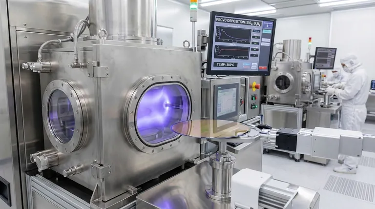
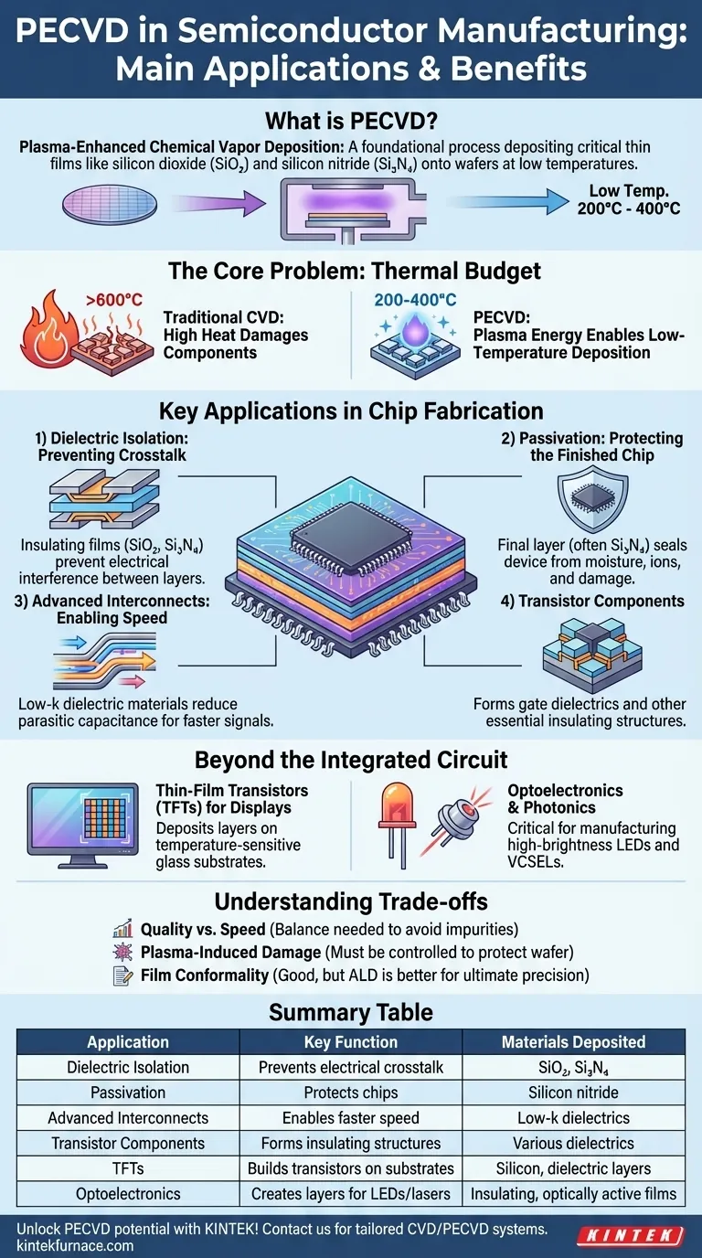
In the semiconductor industry, Plasma-Enhanced Chemical Vapor Deposition (PECVD) is a foundational process used to deposit critical thin films, such as silicon dioxide and silicon nitride, onto wafers. These films serve as essential insulators between conductive layers, protective barriers for the finished chip, and functional components in devices like transistors and LEDs. Its primary advantage is the ability to perform this deposition at low temperatures, preserving the integrity of previously fabricated structures on the chip.
The central value of PECVD is not just what it deposits, but how it does so. By using an energy-rich plasma instead of high heat, it allows manufacturers to build complex, multi-layered microchips without damaging the delicate, temperature-sensitive components already on the wafer.
The Core Problem PECVD Solves: The Thermal Budget
Modern microchips are built vertically, layer by layer. The central challenge is adding new layers without melting or altering the ones beneath. This constraint is known as the thermal budget.
The Limitation of Traditional CVD
Traditional Chemical Vapor Deposition (CVD) relies on high temperatures (often >600°C) to provide the energy needed for chemical reactions to occur and form a film on the wafer surface.
This high heat is incompatible with many stages of modern chip fabrication. Components like aluminum interconnects or precisely doped transistor regions would be destroyed or altered by such temperatures.
How Plasma Enables Low-Temperature Deposition
PECVD bypasses the need for high thermal energy by creating a plasma, an ionized gas containing highly reactive species.
This plasma provides the activation energy for the chemical reactions, allowing high-quality films to be deposited at much lower temperatures, typically between 200°C and 400°C. This effectively solves the thermal budget problem.
Key Applications in Chip Fabrication
PECVD's low-temperature capability makes it indispensable for depositing several types of films throughout the chip manufacturing process.
Dielectric Isolation: Preventing Crosstalk
The most common application of PECVD is depositing insulating films like silicon dioxide (SiO₂) and silicon nitride (Si₃N₄).
These dielectric layers are placed between metal wiring layers to prevent electrical signals from interfering with each other, a phenomenon known as crosstalk. This electrical isolation is fundamental to the function of any integrated circuit.
Passivation: Protecting the Finished Chip
The final layer applied to a chip is often a passivation layer, typically made of silicon nitride.
This durable film acts as a robust barrier, sealing the device from moisture, mobile ions, and physical damage during packaging and operation. This significantly improves the chip's long-term reliability.
Advanced Interconnects: Enabling Speed
In high-performance chips, the speed at which signals travel through wires is critical. PECVD is used to deposit low-k dielectric materials.
These advanced insulators have a lower dielectric constant (k) than traditional SiO₂, reducing parasitic capacitance between adjacent wires. This allows signals to propagate faster and reduces power consumption.
Transistor Components
PECVD is also used to deposit films that become part of the transistor itself, such as gate dielectrics or other insulating structures within the complex, three-dimensional architecture of modern transistors.
Beyond the Integrated Circuit
The utility of PECVD extends to other critical semiconductor devices that share similar manufacturing principles.
Powering Displays with Thin-Film Transistors (TFTs)
Modern LCD and OLED displays rely on a vast matrix of Thin-Film Transistors (TFTs) on a glass substrate to control each pixel.
Because the glass substrate cannot withstand high temperatures, PECVD is the essential method for depositing the silicon and dielectric layers required to build these transistors.
Optoelectronics and Photonics
PECVD is vital for manufacturing optoelectronic devices like high-brightness LEDs and Vertical-Cavity Surface-Emitting Lasers (VCSELs). It is used to deposit insulating, passivating, and optically active layers required for light generation and management.
Understanding the Trade-offs
While powerful, PECVD is not without its compromises. A skilled engineer must balance its benefits against its limitations.
Quality vs. Speed
PECVD offers very high deposition rates, which is excellent for manufacturing throughput. However, running the process too fast can sometimes compromise film quality, leading to lower density or incorporating impurities like hydrogen.
Plasma-Induced Damage
The high-energy plasma that enables low-temperature deposition can also cause physical or electrical damage to the wafer's surface if not carefully controlled. Process parameters must be finely tuned to minimize this effect.
Film Conformality
PECVD provides good conformality, meaning it can coat the sidewalls of deep trenches and complex topographies. However, for the most demanding 3D structures requiring near-perfect, atom-by-atom coverage, other processes like Atomic Layer Deposition (ALD) may be superior, albeit at a much slower pace.
Making the Right Choice for Your Goal
Selecting the right deposition technology depends entirely on the specific requirements of the device you are fabricating.
- If your primary focus is building multi-layered ICs: PECVD is the industry standard for depositing the dielectric and passivation films needed after the first metal layers are in place.
- If your primary focus is ultimate precision and conformality for cutting-edge 3D transistors: Consider a slower but more precise method like ALD for the most critical, atomically thin layers.
- If your primary focus is high-throughput manufacturing for displays or solar cells: PECVD delivers the ideal combination of low-temperature processing, high deposition speed, and sufficient film quality.
Ultimately, PECVD's ability to decouple the deposition process from high heat is what makes the construction of complex, reliable, and powerful modern electronics possible.
Summary Table:
| Application | Key Function | Materials Deposited |
|---|---|---|
| Dielectric Isolation | Prevents electrical crosstalk between metal layers | Silicon dioxide (SiO₂), Silicon nitride (Si₃N₄) |
| Passivation | Protects chips from moisture and damage | Silicon nitride |
| Advanced Interconnects | Enables faster signal speeds with low-k dielectrics | Low-k dielectric materials |
| Transistor Components | Forms insulating structures in transistors | Various dielectric films |
| Thin-Film Transistors (TFTs) | Builds transistors on temperature-sensitive substrates | Silicon and dielectric layers |
| Optoelectronics | Creates layers for LEDs and lasers | Insulating and optically active films |
Unlock the full potential of PECVD for your semiconductor projects with KINTEK! Leveraging exceptional R&D and in-house manufacturing, we provide diverse laboratories with advanced high-temperature furnace solutions, including CVD/PECVD Systems. Our strong deep customization capability ensures precise alignment with your unique experimental requirements, enhancing efficiency and reliability. Contact us today to discuss how our tailored solutions can drive your innovations forward!
Visual Guide
Related Products
- RF PECVD System Radio Frequency Plasma Enhanced Chemical Vapor Deposition
- Slide PECVD Tube Furnace with Liquid Gasifier PECVD Machine
- Inclined Rotary Plasma Enhanced Chemical Deposition PECVD Tube Furnace Machine
- Inclined Rotary Plasma Enhanced Chemical Deposition PECVD Tube Furnace Machine
- Cylindrical Resonator MPCVD Machine System for Lab Diamond Growth
People Also Ask
- What is RF in PECVD? A Critical Control for Plasma Deposition
- How is silicon dioxide deposited from tetraethylorthosilicate (TEOS) in PECVD? Achieve Low-Temperature, High-Quality SiO2 Films
- How does film quality compare between PECVD and CVD? Choose the Best Method for Your Substrate
- How are deposition rates and film properties controlled in PECVD? Master Key Parameters for Optimal Thin Films
- What are the advantages of PECVD in film deposition? Achieve Low-Temp, High-Quality Coatings


