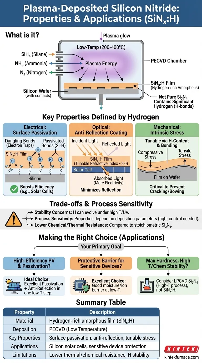
In short, plasma-deposited silicon nitride is not a pure material but a hydrogen-rich amorphous film, typically denoted as SiNₓ:H. It is formed at low temperatures using plasma-enhanced chemical vapor deposition (PECVD) from precursor gases like silane and ammonia. The significant, intentionally incorporated hydrogen content is what defines its most critical properties, making it distinct from pure, stoichiometric silicon nitride (Si₃N₄).
The crucial takeaway is that the value of plasma-deposited silicon nitride comes directly from its manufacturing process. The low-temperature plasma deposition creates a unique, hydrogenated material whose electronic and optical properties can be precisely tuned for specific applications, most notably for improving the efficiency of silicon solar cells.
The Deposition Process: Why "Plasma-Deposited" Matters
The method used to create a material fundamentally defines its structure and properties. This is especially true for plasma-deposited silicon nitride.
The Role of Plasma-Enhanced Chemical Vapor Deposition (PECVD)
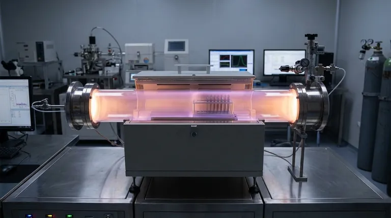
PECVD is a process that uses an energy-rich plasma to break down precursor gases at relatively low temperatures (typically 200-400°C).
This low-temperature nature is a significant advantage, allowing the film to be deposited on substrates that cannot withstand the high temperatures (700-900°C) required for other methods, such as silicon wafers with pre-existing metal contacts.
Precursor Gases and Hydrogen Incorporation
The most common gases used are silane (SiH₄) and ammonia (NH₃), or sometimes nitrogen (N₂). These gases provide the silicon and nitrogen atoms for the film.
Crucially, they also serve as the source for a significant amount of hydrogen, which becomes bonded within the film's structure as Si-H and N-H groups. This is not an impurity; it is a defining and desirable feature of the material.
The Resulting Amorphous Structure
Unlike high-temperature deposition methods that produce a dense, crystalline, and chemically pure silicon nitride (Si₃N₄), PECVD creates an amorphous film.
This means the atoms lack long-range order. The resulting material is more accurately described as hydrogenated amorphous silicon nitride (SiNₓ:H), where 'x' indicates it is not perfectly stoichiometric.
Key Properties Defined by Hydrogen
The embedded hydrogen is not a passive component. It actively shapes the material's most important characteristics, which can be tuned by controlling the deposition parameters.
Electrical Property: Surface Passivation
This is arguably the most important property for semiconductor applications. At the surface of a silicon wafer, there are incomplete chemical bonds ("dangling bonds") that act as traps for electrons, reducing device efficiency.
The hydrogen within the SiNₓ:H film is mobile enough during deposition to diffuse a short distance into the silicon surface. There, it bonds to these dangling bonds, electrically "passivating" or neutralizing them. This dramatically improves the performance of devices like solar cells.
Optical Property: Anti-Reflection Coating
By carefully controlling the gas ratios during deposition, the refractive index of the SiNₓ:H film can be tuned (typically to around 2.0).
This allows the film to function as an excellent anti-reflection coating on silicon. A quarter-wavelength thick layer minimizes light reflection from the solar cell's surface, maximizing the amount of light absorbed and converted into electricity.
Mechanical Property: Intrinsic Stress
All thin films possess some level of internal stress. The hydrogen content and bonding configuration in SiNₓ:H directly influence this stress, which can be engineered to be either compressive or tensile.
Managing this stress is critical to prevent the film from cracking or causing the underlying wafer to bow, ensuring the mechanical integrity of the final device.
Understanding the Trade-offs
While highly useful, plasma-deposited silicon nitride is not a universally perfect solution. Its unique nature comes with specific limitations.
Stability Concerns
The beneficial hydrogen can also be a point of weakness. Under prolonged exposure to high temperatures or intense ultraviolet (UV) light, the hydrogen can evolve out of the film.
This can alter the film's passivation quality, optical properties, and stress over the lifetime of the device, leading to potential performance degradation if not properly managed.
Process Sensitivity
The properties of SiNₓ:H are not fixed; they are a direct function of the deposition parameters (temperature, pressure, gas flow rates, plasma power).
This makes process control absolutely critical. Minor variations can lead to significant changes in the final film, requiring tight manufacturing discipline to ensure consistency and repeatability.
Lower Chemical and Thermal Resistance
Compared to high-temperature, stoichiometric Si₃N₄, plasma-deposited SiNₓ:H is generally less dense and less chemically inert. It cannot withstand the same extreme temperatures or harsh chemical environments.
Making the Right Choice for Your Goal
Your choice of material depends entirely on the primary goal of your application.
- If your primary focus is high-efficiency silicon photovoltaics: This is the ideal material, as it uniquely provides both excellent surface passivation and an anti-reflection coating in a single, low-temperature deposition step.
- If your primary focus is a protective barrier on a temperature-sensitive device: Its good performance as a moisture and ion barrier, combined with the low-temperature process, makes it an excellent choice for encapsulation.
- If your primary focus is maximum hardness, thermal stability, or resistance to harsh chemicals: You should consider a stoichiometric silicon nitride made via a high-temperature process like Low-Pressure CVD (LPCVD), as plasma-deposited SiN is not optimized for these extremes.
Ultimately, choosing plasma-deposited silicon nitride is a decision to leverage a tunable, process-defined material for its unique electronic and optical benefits at low temperatures.
Summary Table:
| Property | Description |
|---|---|
| Material Type | Hydrogen-rich amorphous film (SiNₓ:H) |
| Deposition Method | Plasma-Enhanced Chemical Vapor Deposition (PECVD) |
| Key Properties | Surface passivation, anti-reflection coating, tunable stress |
| Common Applications | Silicon solar cells, temperature-sensitive device protection |
| Limitations | Lower thermal/chemical resistance, hydrogen stability concerns |
Unlock the potential of plasma-deposited silicon nitride for your lab with KINTEK! We specialize in advanced high-temperature furnace solutions, including PECVD Systems, tailored to meet your unique experimental needs. Our expertise in R&D and in-house manufacturing ensures precise customization for applications like solar cell development. Contact us today to discuss how we can enhance your research and production processes with reliable, high-performance equipment.
Visual Guide
Related Products
- MPCVD Machine System Reactor Bell-jar Resonator for Lab and Diamond Growth
- Slide PECVD Tube Furnace with Liquid Gasifier PECVD Machine
- RF PECVD System Radio Frequency Plasma Enhanced Chemical Vapor Deposition
- Inclined Rotary Plasma Enhanced Chemical Deposition PECVD Tube Furnace Machine
- Inclined Rotary Plasma Enhanced Chemical Deposition PECVD Tube Furnace Machine
People Also Ask
- What are the key components of an MPCVD system? Unlock High-Purity Crystal Growth
- What role does gas flow rate play in MPCVD? Mastering Deposition Rate and Film Uniformity
- How can the growth rate of diamond be accelerated in the MPCVD method? Boost Growth with Higher Power & Pressure
- What are future trends in MPCVD technology? Unlock Next-Gen Materials with AI and Efficiency
- How does pressure affect the MPCVD growth process? Master Plasma Control for Superior Film Quality


