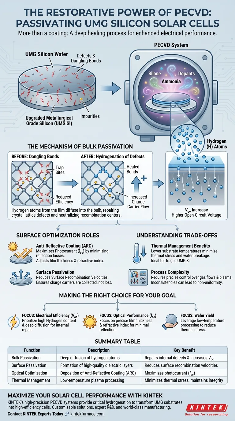
The primary function of a Plasma Enhanced Chemical Vapor Deposition (PECVD) system in processing upgraded metallurgical grade (UMG) silicon is to deposit thin films of silicon nitride, silicon oxide, or silicon oxynitride onto the wafer surface.
While these films serve as an optical anti-reflective coating, their most critical role is bulk passivation. The process introduces hydrogen atoms into the silicon structure, which repair internal defects and dangling bonds, directly improving the solar cell's electrical performance.
Core Insight: For upgraded metallurgical grade silicon, PECVD is not just about surface coating; it is a restorative process. The system drives hydrogen atoms deep into the wafer to neutralize atomic defects, which is the primary driver for increasing the cell's open-circuit voltage ($V_{oc}$).
The Mechanism of Bulk Passivation
Hydrogenation of Defects
Upgraded metallurgical grade silicon typically contains higher levels of impurities and crystal defects than semiconductor-grade silicon. These defects create dangling bonds—broken atomic connections that trap electrons and reduce efficiency.
Repairing the Crystal Lattice
During the PECVD process, the deposition of the silicon nitride or oxide layer releases hydrogen atoms. These atoms diffuse from the surface coating into the bulk of the silicon wafer.
Once inside, the hydrogen binds with the dangling bonds, effectively "healing" the defects. This prevents charge carriers (electrons and holes) from recombining prematurely at these defect sites.
Increasing Open-Circuit Voltage
The direct result of this hydrogen passivation is a significant increase in the open-circuit voltage ($V_{oc}$). By neutralizing the internal recombination centers, the PECVD process ensures that the inherent quality of the lower-cost UMG silicon does not compromise the final energy output of the cell.
Surface Optimization Roles
Anti-Reflective Coating (ARC)
Beyond internal repair, the thin films deposited by PECVD (specifically silicon nitride) act as an anti-reflective coating.
By adjusting the thickness and refractive index of the film, the system ensures that more incoming sunlight enters the cell rather than bouncing off the surface. This maximizes the photocurrent generated by the device.
Surface Passivation
In addition to bulk passivation, the deposited stack also passivates the surface of the wafer. This reduces surface recombination velocities, ensuring that charge carriers generated near the surface are collected rather than lost.
Understanding the Trade-offs
Thermal Management Benefits
A distinct advantage of PECVD over standard thermal CVD is its ability to operate at lower substrate temperatures.
Because the energy required for the chemical reaction is supplied by the plasma rather than heat alone, the process minimizes thermal stress on the silicon wafer. This is crucial for maintaining the structural integrity of the substrate and preventing the activation of certain heat-sensitive impurities found in UMG silicon.
Process Complexity
However, PECVD requires precise control over gas flows (such as silane, ammonia, or dopant gases) and plasma conditions. Inconsistencies in the plasma can lead to non-uniform film thickness or "blooming effects," which can alter the passivation quality or optical properties of the cell.
Making the Right Choice for Your Goal
When evaluating PECVD processes for UMG silicon, consider your specific performance targets:
- If your primary focus is Electrical Efficiency ($V_{oc}$): Prioritize process parameters that maximize hydrogen content in the film and facilitate its diffusion into the bulk silicon to repair internal defects.
- If your primary focus is Optical Performance ($I_{sc}$): Focus on the precise control of film thickness and refractive index to minimize reflection losses across the solar spectrum.
- If your primary focus is Wafer Yield: Leverage the low-temperature capabilities of PECVD to reduce thermal stress and prevent breakage of fragile substrates.
Ultimately, the effectiveness of a PECVD system is measured by its ability to balance surface optics with the deep, restorative hydrogenation required by upgraded metallurgical grade silicon.
Summary Table:
| Function | Description | Key Benefit |
|---|---|---|
| Bulk Passivation | Deep diffusion of hydrogen atoms into the wafer | Repairs internal defects & increases $V_{oc}$ |
| Surface Passivation | Formation of high-quality dielectric layers | Reduces surface recombination velocities |
| Optical Optimization | Deposition of Anti-Reflective Coating (ARC) | Maximizes photocurrent ($I_{sc}$) by reducing reflection |
| Thermal Management | Low-temperature plasma processing | Minimizes thermal stress and maintains wafer integrity |
Maximize Your Solar Cell Performance with KINTEK
Is your UMG silicon reaching its full potential? KINTEK’s high-precision PECVD systems provide the critical hydrogenation needed to transform low-cost substrates into high-efficiency solar cells. Backed by expert R&D and world-class manufacturing, we offer a comprehensive range of Muffle, Tube, Rotary, Vacuum, and CVD/PECVD systems—all fully customizable to meet your unique lab or production requirements.
Don't let impurities limit your output. Our specialized high-temperature solutions ensure uniform film deposition and superior bulk passivation for any material science application.
Contact KINTEK Experts Today to discover how our customizable furnace technology can elevate your research and production efficiency.
Visual Guide
References
- Production of upgraded metallurgical-grade silicon for a low-cost, high-efficiency, and reliable PV technology. DOI: 10.3389/fphot.2024.1331030
This article is also based on technical information from Kintek Furnace Knowledge Base .
Related Products
- RF PECVD System Radio Frequency Plasma Enhanced Chemical Vapor Deposition
- Slide PECVD Tube Furnace with Liquid Gasifier PECVD Machine
- Inclined Rotary Plasma Enhanced Chemical Deposition PECVD Tube Furnace Machine
- Inclined Rotary Plasma Enhanced Chemical Deposition PECVD Tube Furnace Machine
- MPCVD Machine System Reactor Bell-jar Resonator for Lab and Diamond Growth
People Also Ask
- What are the key advantages of PECVD technology? Achieve Low-Temperature, High-Quality Thin Film Deposition
- What are some promising applications of PECVD-prepared 2D materials? Unlock Advanced Sensing and Optoelectronics
- What is RF in PECVD? A Critical Control for Plasma Deposition
- What are the advantages of PECVD in film deposition? Achieve Low-Temp, High-Quality Coatings
- What are the limitations of PECVD? Overcome Process Control and Cost Challenges


