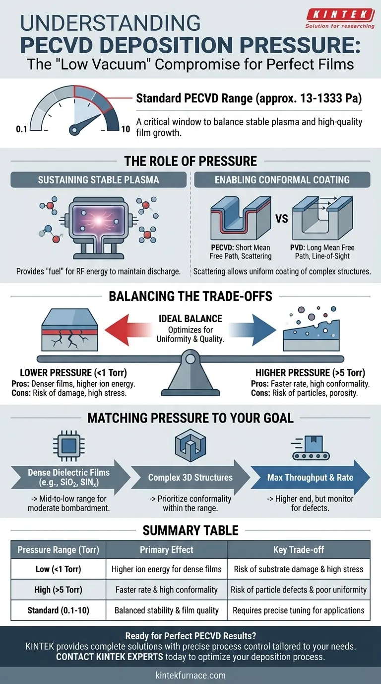
In a standard PECVD process, the chamber pressure is typically maintained in a "low vacuum" range, most often between 0.1 and 10 Torr (approximately 13 to 1333 Pascals). This specific pressure window is not arbitrary; it is a critical parameter engineered to balance the need for a stable plasma with the requirements for high-quality, uniform film growth.
The operating pressure in PECVD is a deliberate compromise. It is high enough to sustain a dense, reactive plasma for uniform, conformal coating, but low enough to prevent unwanted gas-phase reactions and particle formation that would otherwise degrade the resulting film.
The Role of Pressure in the PECVD Process
To understand PECVD, you must understand why this pressure range is essential. It directly controls the environment where the film is created, influencing everything from reaction chemistry to the physical properties of the final layer.
Sustaining a Stable Plasma
A plasma is a gas of ionized particles. To create and sustain it with radio-frequency (RF) power, you need a sufficient density of gas molecules to ionize.
Pressures in the 0.1 to 10 Torr range provide enough "fuel" for the RF energy to maintain a stable, glowing plasma discharge throughout the chamber, which is the engine of the deposition process.
Enabling Conformal Coating
The pressure dictates the mean free path—the average distance a gas molecule travels before colliding with another. In the PECVD pressure range, the mean free path is short.
This means reactive chemical species created in the plasma will scatter and collide many times before reaching the substrate. This scattering effect is highly desirable, as it allows the precursors to coat all surfaces uniformly, including the sides and bottoms of complex 3D trenches. This is known as conformal coating.
Contrasting with "Line-of-Sight" Deposition
This behavior is a key advantage over lower-pressure techniques like Physical Vapor Deposition (PVD), which operate in a high vacuum (<10⁻³ Torr).
In PVD, the mean free path is very long, so coating atoms travel in straight lines from the source to the substrate. This "line-of-sight" deposition makes it difficult to coat complex, non-visible surfaces effectively.
Understanding the Trade-offs of PECVD Pressure
Adjusting the pressure within the operational window is a primary method for tuning film properties. However, it involves critical trade-offs that every engineer must consider.
Pressure vs. Film Quality
Operating at the lower end of the pressure range (e.g., < 1 Torr) can increase the energy of ions striking the substrate. This bombardment can create denser, more robust films, but it can also induce compressive stress and potentially cause substrate damage.
Conversely, operating at the higher end (e.g., > 5 Torr) reduces ion energy but increases the risk of gas-phase nucleation, where particles form in the plasma itself. These particles can fall onto the wafer, creating defects and increasing film porosity.
Pressure vs. Deposition Rate
Generally, a higher pressure means more reactant gas molecules are available, which can lead to a faster deposition rate.
However, this is not a linear relationship. Pushing the pressure too high can lead to the aforementioned quality issues or inefficient plasma coupling, potentially causing the deposition rate to plateau or even decrease.
Pressure vs. Uniformity
The ideal pressure helps ensure the reactive gas species are distributed evenly across the entire substrate surface before they deposit.
If the pressure is too low, the plasma may not be uniform. If it's too high, reactions can occur too quickly near the gas inlet, leading to a "depletion effect" where the film is thicker on one side of the substrate than the other.
Matching the Pressure to Your Deposition Goal
The optimal pressure setting is entirely dependent on the desired outcome for your specific material and application. Use the following as a guide.
- If your primary focus is high-quality, dense dielectric films (e.g., SiO₂, SiNₓ): You will likely operate in a well-characterized mid-to-low pressure range to leverage moderate ion bombardment for densification while avoiding damage.
- If your primary focus is coating complex 3D structures: PECVD's inherent "low vacuum" operation is advantageous, and you would prioritize a pressure that maximizes conformality without creating voids.
- If your primary focus is maximizing throughput and deposition rate: You may push toward the higher end of the pressure range, but you must carefully monitor film quality for particle defects and non-uniformity.
Ultimately, pressure is the most fundamental control knob you have for tuning the balance between deposition rate, film quality, and uniformity.
Summary Table:
| Pressure Range (Torr) | Primary Effect | Key Trade-off |
|---|---|---|
| Low (e.g., < 1 Torr) | Higher ion energy for denser films | Risk of substrate damage and high stress |
| High (e.g., > 5 Torr) | Faster deposition rate & high conformality | Risk of particle defects and poor uniformity |
| Standard (0.1 - 10 Torr) | Balanced plasma stability & film quality | Requires precise tuning for specific applications |
Ready to Achieve Perfect PECVD Results?
The ideal pressure is just one parameter in a complex process. At KINTEK, we don't just sell furnaces; we provide complete solutions. Our deep expertise in CVD/PECVD Systems, combined with our exceptional in-house R&D and manufacturing capabilities, allows us to deliver systems with precise process control tailored to your unique materials and application requirements—whether you need superior conformality for 3D structures or dense, high-quality dielectric films.
Contact our experts today to discuss how a KINTEK PECVD system can be customized to optimize your deposition process and accelerate your R&D.
Visual Guide
Related Products
- RF PECVD System Radio Frequency Plasma Enhanced Chemical Vapor Deposition
- Slide PECVD Tube Furnace with Liquid Gasifier PECVD Machine
- Inclined Rotary Plasma Enhanced Chemical Deposition PECVD Tube Furnace Machine
- Inclined Rotary Plasma Enhanced Chemical Deposition PECVD Tube Furnace Machine
- Cylindrical Resonator MPCVD Machine System for Lab Diamond Growth
People Also Ask
- How does film quality compare between PECVD and CVD? Choose the Best Method for Your Substrate
- What are the advantages of PECVD in film deposition? Achieve Low-Temp, High-Quality Coatings
- How are deposition rates and film properties controlled in PECVD? Master Key Parameters for Optimal Thin Films
- What is the role of RF power in PECVD and how does the RF-PECVD process work? Master Thin Film Deposition Control
- What is RF in PECVD? A Critical Control for Plasma Deposition


