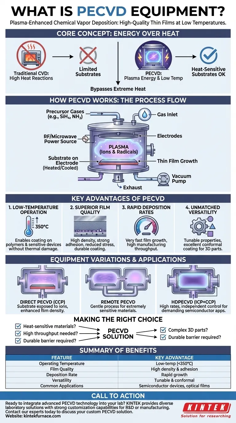
At its core, Plasma-Enhanced Chemical Vapor Deposition (PECVD) equipment is a system designed to deposit high-quality thin films onto a substrate. Unlike traditional Chemical Vapor Deposition (CVD) which relies on high temperatures to drive chemical reactions, PECVD uses an energized plasma to achieve deposition at significantly lower temperatures, making it indispensable for modern materials engineering.
The fundamental advantage of PECVD is its ability to bypass the need for extreme heat. By using plasma to break down precursor gases, it enables the creation of high-performance thin films on materials that would otherwise be damaged or destroyed by conventional high-temperature processes.
How PECVD Works: Using Energy Instead of Heat
To understand the equipment, you must first understand the process. PECVD manipulates chemistry within a vacuum by introducing energy in the form of plasma.
The Core Components
A PECVD system is fundamentally a controlled environment. It consists of a vacuum chamber to remove atmospheric contaminants, gas inlets to introduce precise amounts of precursor gases, and a set of electrodes.
These electrodes are connected to a radio frequency (RF) or microwave power source, which is the engine that creates the plasma. The substrate sits on one of the electrodes, which can often be heated or cooled to fine-tune the process.
The Plasma-Enhanced Process
The process begins by placing a substrate inside the chamber and creating a vacuum. Precursor gases, such as silane (SiH₄) and ammonia (NH₃) for silicon nitride films, are then introduced.
Next, the RF power source is activated, creating a powerful electric field between the electrodes. This field energizes the gas, stripping electrons from the atoms and creating a glowing, ionized gas known as plasma.
Within this plasma, highly reactive ions and radicals are formed at a low overall temperature. These reactive species then bombard the substrate surface, where they react and bond to form a dense, uniform thin film.
Key Advantages of the PECVD Method
Choosing PECVD is often a strategic decision driven by its unique combination of benefits that are difficult to achieve with other methods like Physical Vapor Deposition (PVD) or high-temperature CVD.
Low-Temperature Operation
This is the defining feature of PECVD. By operating at lower temperatures (often below 350°C), it allows for deposition on temperature-sensitive substrates like polymers, plastics, and certain semiconductor devices without causing thermal damage.
Superior Film Quality
PECVD films are known for their excellent quality. They exhibit high density with fewer pinholes, strong adhesion to the substrate, and reduced internal stress, which makes them less prone to cracking. The result is a more durable and reliable coating.
Rapid Deposition Rates
The high reactivity of the species within the plasma leads to very fast film growth. For some materials, such as silicon nitride, deposition rates can be over 160 times faster than conventional CVD, enabling higher throughput in manufacturing environments.
Unmatched Versatility
The process is incredibly flexible. By adjusting gas composition, pressure, and plasma power, engineers can precisely tune the film's properties, such as its chemical resistance or optical characteristics. It is also excellent for coating complex, three-dimensional surfaces uniformly.
Understanding PECVD Equipment Variations
Not all PECVD systems are the same. The specific design of the reactor dictates its capabilities and ideal applications. Understanding these differences is key to selecting the right tool.
Direct vs. Remote Plasma Reactors
Direct PECVD, also known as capacitively coupled plasma (CCP), is the most common configuration. The substrate is placed directly within the plasma, exposing it to both chemical species and ion bombardment, which can enhance film density.
Remote PECVD generates the plasma in a separate chamber. Only the chemically reactive species flow to the substrate, not the high-energy ions. This gentler process is ideal for depositing films on extremely sensitive electronic materials where ion-induced damage must be avoided.
High-Density PECVD (HDPECVD)
This advanced technique combines an inductively coupled plasma (ICP) source to create a very dense plasma with a separate, capacitively coupled bias on the substrate. HDPECVD offers higher deposition rates and gives independent control over film properties, making it a powerful tool for demanding semiconductor applications.
Common Pitfalls and Considerations
While powerful, PECVD is not a universal solution. The equipment is complex and operates under a vacuum, requiring significant capital investment and maintenance. The "semi-clean" nature of some tools means they may not be suitable for the most stringent, ultra-high-purity semiconductor fabrication lines without specific design considerations.
Making the Right Choice for Your Application
Your specific goal determines whether PECVD is the correct technology for your project.
- If your primary focus is depositing on heat-sensitive materials: PECVD is the clear and often only choice due to its low-temperature capabilities.
- If your primary focus is manufacturing throughput: PECVD's rapid deposition rates offer a significant advantage over many other thin-film techniques.
- If your primary focus is coating complex 3D parts: The conformal nature of PECVD deposition provides uniform coverage that is difficult to achieve with line-of-sight PVD methods.
- If your primary focus is creating a high-quality, durable barrier: The dense, non-porous, and crack-resistant films from PECVD are ideal for protective and anti-corrosion applications.
Ultimately, PECVD equipment empowers you to create advanced materials that would be impossible to fabricate with heat alone.
Summary Table:
| Feature | Key Advantage |
|---|---|
| Operating Temperature | Low-temperature process (< 350°C), ideal for heat-sensitive substrates |
| Film Quality | High density, strong adhesion, and reduced internal stress |
| Deposition Rate | Rapid film growth, significantly faster than conventional CVD |
| Versatility | Tunable film properties and excellent conformal coating for 3D parts |
| Common Applications | Semiconductor devices, protective coatings, optical films, MEMS |
Ready to integrate advanced PECVD technology into your lab?
Leveraging exceptional R&D and in-house manufacturing, KINTEK provides diverse laboratories with advanced high-temperature furnace and thin-film deposition solutions. Our PECVD systems are complemented by our strong deep customization capability to precisely meet your unique experimental requirements, whether for R&D or high-throughput manufacturing.
Contact our experts today to discuss how a custom PECVD solution can advance your materials engineering projects.
Visual Guide
Related Products
- Slide PECVD Tube Furnace with Liquid Gasifier PECVD Machine
- Inclined Rotary Plasma Enhanced Chemical Deposition PECVD Tube Furnace Machine
- Inclined Rotary Plasma Enhanced Chemical Deposition PECVD Tube Furnace Machine
- RF PECVD System Radio Frequency Plasma Enhanced Chemical Vapor Deposition
- Multi Heating Zones CVD Tube Furnace Machine for Chemical Vapor Deposition Equipment
People Also Ask
- What are the typical conditions for plasma-enhanced CVD processes? Achieve Low-Temperature Thin Film Deposition
- What are the main advantages of PECVD tube furnaces compared to CVD tube furnaces? Lower Temp, Faster Deposition, and More
- What plasma source is used in PE-CVD tube furnaces? Unlock Low-Temperature, High-Quality Deposition
- What are the disadvantages of tube furnace cracking when processing heavy raw materials? Avoid Costly Downtime and Inefficiency
- How does PECVD equipment contribute to TOPCon bottom cells? Mastering Hydrogenation for Maximum Solar Efficiency


