In modern semiconductor fabrication, PECVD is uniquely suitable because it allows for the deposition of high-quality insulating and protective films at low temperatures. This capability is essential for building complex, multi-layered microchips without damaging the fragile, temperature-sensitive components already fabricated on the silicon wafer.
PECVD’s primary advantage is that it decouples the energy required for chemical reactions from thermal energy. By using an energized plasma rather than high heat, it enables the creation of critical device layers that would be impossible to form with traditional high-temperature methods.
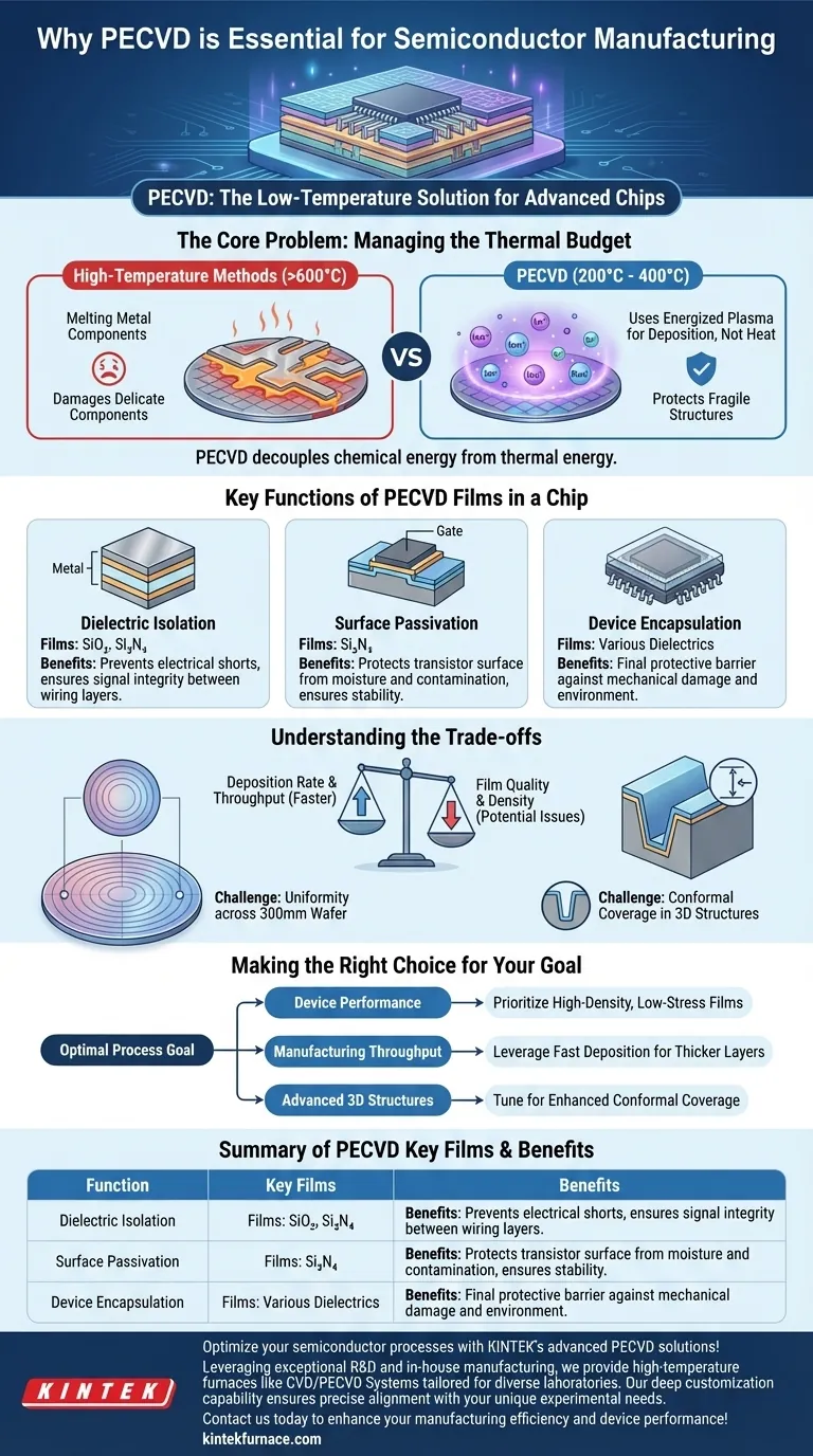
The Core Problem: Managing the Thermal Budget
The fabrication of a semiconductor device involves hundreds of sequential steps. A critical constraint governing this entire process is the "thermal budget"—the total amount of high-temperature processing a wafer can endure before its delicate structures are compromised.
Why High Temperatures Are a Deal-Breaker
Once components like transistors and their initial metal wiring are formed, the wafer becomes extremely sensitive to heat.
Exposing it to high temperatures again can cause metal layers to melt, dopants to diffuse out of their precise locations, and carefully engineered junctions to fail. This would effectively destroy the device.
How Plasma Provides Energy Without Heat
Traditional Chemical Vapor Deposition (CVD) relies on high temperatures (often >600°C) to provide the energy needed to break down precursor gases and deposit a film.
Plasma-Enhanced CVD (PECVD) circumvents this by using a radio frequency (RF) field to ignite a plasma. This plasma contains highly reactive ions and radicals that can drive the deposition reaction at much lower substrate temperatures, typically between 200°C and 400°C.
Key Functions of PECVD Films in a Chip
PECVD is not just a single-use tool; it is a versatile workhorse used to deposit various films that serve distinct, critical functions within the integrated circuit.
Dielectric Isolation
The most common use of PECVD is to deposit dielectric (electrically insulating) films like silicon dioxide (SiO₂) and silicon nitride (Si₃N₄).
These layers are deposited between the multiple layers of metal wiring in a chip, preventing electrical shorts and ensuring signals travel along their intended paths without interference.
Surface Passivation
The silicon surface at the heart of a transistor is highly sensitive to its chemical and electrical environment.
A PECVD-deposited film, often silicon nitride, is used to "passivate" this surface. This layer protects the active regions of the transistor from moisture and ionic contamination, ensuring long-term stability and reliability.
Device Encapsulation
As a final protective step, PECVD is used to encapsulate the entire integrated circuit. This final passivation layer acts as a robust physical barrier, sealing the device from the outside world and protecting it from mechanical damage and environmental exposure.
Understanding the Trade-offs
While indispensable, PECVD is not without its engineering challenges and compromises. Objectively understanding these limitations is key to its successful implementation.
Film Quality vs. Deposition Rate
PECVD offers significantly faster deposition rates compared to other low-temperature methods, which is a major advantage for manufacturing throughput.
However, there is often a trade-off. Pushing for the highest possible speed can sometimes result in a less dense film or the inclusion of more hydrogen atoms, which can affect its electrical properties.
The Challenge of Uniformity
Achieving a perfectly uniform film thickness across a large 300mm wafer is a constant process engineering challenge. Non-uniformity can impact the performance and yield of devices across the wafer.
Conformal Coverage
Conformality refers to a film's ability to cover the vertical sidewalls of a feature as thickly as it covers the horizontal surfaces. While PECVD offers good conformality for many applications, it can struggle with the extremely deep, narrow trenches found in advanced 3D structures.
Making the Right Choice for Your Goal
The optimal PECVD process depends entirely on the specific requirements of the device layer being created.
- If your primary focus is device performance: Prioritize recipes that yield high-density, low-stress dielectric films for superior isolation and passivation.
- If your primary focus is manufacturing throughput: Leverage PECVD's fast deposition rates for thicker, less critical layers like final encapsulation, where minor variations are acceptable.
- If your primary focus is advanced 3D structures: Tune the process parameters to enhance conformal coverage, even if it means accepting a slightly slower deposition rate.
Ultimately, PECVD's mastery lies in its ability to solve a fundamental conflict, making it an indispensable tool for balancing device performance with manufacturing efficiency.
Summary Table:
| Function | Key Films | Benefits |
|---|---|---|
| Dielectric Isolation | SiO₂, Si₃N₄ | Prevents electrical shorts, ensures signal integrity |
| Surface Passivation | Si₃N₄ | Protects transistors from moisture and contamination |
| Device Encapsulation | Various dielectrics | Seals chips from mechanical and environmental damage |
Optimize your semiconductor processes with KINTEK's advanced PECVD solutions! Leveraging exceptional R&D and in-house manufacturing, we provide high-temperature furnaces like CVD/PECVD Systems tailored for diverse laboratories. Our deep customization capability ensures precise alignment with your unique experimental needs, from dielectric isolation to device encapsulation. Contact us today to discuss how our technology can enhance your manufacturing efficiency and device performance!
Visual Guide
Related Products
- Slide PECVD Tube Furnace with Liquid Gasifier PECVD Machine
- RF PECVD System Radio Frequency Plasma Enhanced Chemical Vapor Deposition
- Inclined Rotary Plasma Enhanced Chemical Deposition PECVD Tube Furnace Machine
- Inclined Rotary Plasma Enhanced Chemical Deposition PECVD Tube Furnace Machine
- Multi Heating Zones CVD Tube Furnace Machine for Chemical Vapor Deposition Equipment
People Also Ask
- How does PECVD equipment contribute to TOPCon bottom cells? Mastering Hydrogenation for Maximum Solar Efficiency
- What are the main advantages of PECVD tube furnaces compared to CVD tube furnaces? Lower Temp, Faster Deposition, and More
- What are the advantages of using a tube furnace CVD system for Cu(111)/graphene? Superior Scalability and Quality
- What are the typical conditions for plasma-enhanced CVD processes? Achieve Low-Temperature Thin Film Deposition
- How does a hydrogen reduction environment in an industrial tube furnace facilitate gold-copper alloy microspheres?


