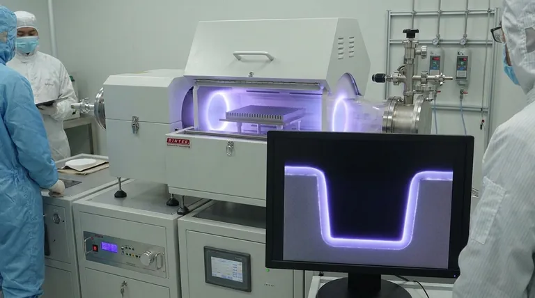
In thin-film deposition, step coverage is a critical metric that defines how uniformly a deposited film conforms to the underlying topography of a substrate. For Plasma-Enhanced Chemical Vapor Deposition (PECVD), it measures the film's ability to maintain its thickness over sharp steps, deep trenches, and other complex, three-dimensional features. This quality is not merely a geometric curiosity; it is a fundamental requirement for the function and reliability of modern microelectronic devices.
The core challenge of step coverage is overcoming geometric "shadowing." Think of it as the difference between spray painting a complex object from one direction versus submerging it in a vat of paint. PECVD aims for the latter, ensuring every nook and cranny receives a uniform coating, which is essential for preventing electrical failures and structural weaknesses in microscopic circuits.
The Mechanics of Step Coverage in PECVD
To understand why step coverage is so crucial, we must first examine how it is achieved and what factors influence it. It's a delicate balance between the directionality of depositing species and their ability to move once they land on the surface.
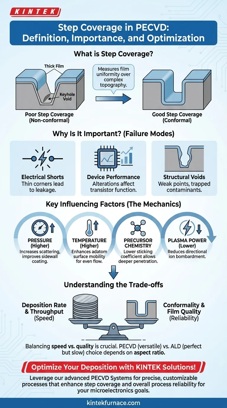
What Defines "Good" vs. "Poor" Step Coverage?
The quality of step coverage is typically described by its conformality. A perfectly conformal film has 100% step coverage, meaning its thickness is identical on the top, bottom, and sidewalls of a feature.
Poor step coverage is non-conformal. This often results in a film that is thick on top surfaces, thinner on the sidewalls, and thinnest (or absent) at the bottom corners of a trench. In extreme cases, this can lead to voids or "keyholes" as the top of the feature closes off before the bottom is fully filled.
The Role of Plasma in Aiding Deposition
Unlike purely thermal processes, PECVD uses a plasma to create reactive chemical species at lower temperatures. This has a mixed effect on step coverage.
The plasma creates a higher concentration of reactive radicals, which can improve deposition in shadowed regions. However, it also creates an electric field that can accelerate ions toward the substrate, leading to a more directional, line-of-sight deposition that can worsen shadowing effects. The key is to balance these competing mechanisms.
Key Influencing Factors
Achieving good step coverage requires precise control over several process parameters.
-
Pressure: Higher process pressure increases gas-phase collisions, making the arrival of film precursors more random and less directional. This scattering effect significantly improves the film's ability to coat sidewalls.
-
Temperature: Increasing the substrate temperature enhances the surface mobility of deposited atoms (adatoms). This allows them to "flow" across the surface after landing, migrating from high-concentration areas (like top corners) into low-concentration areas (like the bottom of a trench), evening out the film thickness.
-
Precursor Gas Chemistry: The choice of precursor gas is vital. Molecules with a longer lifetime and lower sticking coefficient (the probability of sticking upon collision) are more likely to bounce around within a feature before reacting, leading to better conformality.
-
Plasma Power and Frequency: Lowering RF power can reduce ion bombardment and its associated directionality, improving coverage. The frequency of the plasma (low vs. high) also changes the ion energy distribution, providing another lever for process optimization.
Why Poor Step Coverage Is a Critical Failure Mode
In semiconductor manufacturing, a seemingly small defect in step coverage can have catastrophic consequences for the entire device.
Ensuring Electrical Isolation
Dielectric films, such as silicon dioxide (SiO₂), are used to insulate conductive layers. If the step coverage is poor, the film will be dangerously thin at the corners of metal lines. This creates weak spots that can lead to current leakage or a complete electrical short, rendering the circuit useless.
Maintaining Device Performance
Modern transistors, like FinFETs, have complex 3D architectures. The gate dielectric must wrap around the transistor's "fin" with perfect uniformity. Any thinning of this critical layer due to poor step coverage will alter the transistor's electrical properties, leading to unpredictable performance and premature device failure.
Preventing Structural Voids
As non-conformal films build up, the top corners of a trench grow faster than the bottom. This can cause the top of the trench to pinch off, sealing a void or keyhole inside the film. These voids are structural weak points that can trap contaminants and compromise the mechanical integrity of the device.
Understanding the Trade-offs
Optimizing for perfect step coverage does not come without costs. Engineers must balance conformality against other critical manufacturing metrics.
Deposition Rate vs. Conformality
The process conditions that favor excellent step coverage—such as high pressure and low power—often result in a slower deposition rate. In high-volume manufacturing, this trade-off directly impacts throughput and cost. A balance must be struck that meets the device's minimum reliability requirements while maximizing production speed.
Film Quality vs. Coverage
Altering temperature and plasma conditions to improve surface mobility can also change the film's intrinsic properties, such as its density, chemical composition, and mechanical stress. An aggressive process designed solely for coverage might produce a film that is too stressed, leading to cracking or delamination later on.
PECVD vs. Alternative Methods
While PECVD is a versatile workhorse, it has its limits. For the most demanding, highest-aspect-ratio features in advanced logic and memory chips, other methods are often required. Atomic Layer Deposition (ALD), for example, offers nearly perfect 100% step coverage by its very nature, but at a significantly lower deposition rate than PECVD.
Making the Right Choice for Your Goal
Your approach to step coverage should be dictated by the specific requirements of your application.
- If your primary focus is rapid coating of simple, planar surfaces: You can prioritize a high deposition rate, as step coverage is not a significant concern.
- If your primary focus is insulating features with moderate aspect ratios (e.g., 2:1): A well-optimized PECVD process balancing pressure, temperature, and rate will be your most effective solution.
- If your primary focus is flawless conformality in high-aspect-ratio trenches (e.g., >10:1): You must prioritize conditions that enhance surface mobility and reduce directionality, even at the cost of throughput, and may need to evaluate ALD as a necessary alternative.
Mastering the principles of step coverage is fundamental to fabricating reliable, high-performance microstructures.
Summary Table:
| Aspect | Description |
|---|---|
| Definition | Uniformity of film thickness over substrate topography, such as steps and trenches. |
| Importance | Prevents electrical shorts, ensures device reliability, and maintains structural integrity in microelectronics. |
| Key Factors | Pressure, temperature, precursor gas chemistry, plasma power, and frequency influence step coverage. |
| Trade-offs | Balance between deposition rate, film quality, and conformality; PECVD vs. ALD for high-aspect-ratio features. |
Optimize your thin-film deposition with KINTEK's advanced solutions! Leveraging exceptional R&D and in-house manufacturing, we provide diverse laboratories with high-temperature furnace systems like Muffle, Tube, Rotary Furnaces, Vacuum & Atmosphere Furnaces, and CVD/PECVD Systems. Our strong deep customization capability ensures precise alignment with your unique experimental needs, enhancing step coverage and overall process reliability. Contact us today to discuss how we can support your microelectronics fabrication goals!
Visual Guide
Related Products
- Slide PECVD Tube Furnace with Liquid Gasifier PECVD Machine
- RF PECVD System Radio Frequency Plasma Enhanced Chemical Vapor Deposition
- Inclined Rotary Plasma Enhanced Chemical Deposition PECVD Tube Furnace Machine
- Inclined Rotary Plasma Enhanced Chemical Deposition PECVD Tube Furnace Machine
- Multi Heating Zones CVD Tube Furnace Machine for Chemical Vapor Deposition Equipment
People Also Ask
- How does a hydrogen reduction environment in an industrial tube furnace facilitate gold-copper alloy microspheres?
- What are the typical conditions for plasma-enhanced CVD processes? Achieve Low-Temperature Thin Film Deposition
- How does PECVD equipment contribute to TOPCon bottom cells? Mastering Hydrogenation for Maximum Solar Efficiency
- What plasma source is used in PE-CVD tube furnaces? Unlock Low-Temperature, High-Quality Deposition
- What is plasma in the context of PECVD? Unlock Low-Temperature Thin Film Deposition


