In the world of microelectronics, Plasma-Enhanced Chemical Vapor Deposition (PECVD) is a cornerstone technology that enables the fabrication of modern integrated circuits. Its primary benefit is the ability to deposit high-quality, protective thin films at significantly lower temperatures than traditional methods. This low-temperature capability is essential for building complex, multi-layered devices without damaging the fragile, pre-existing components on the silicon wafer.
The core challenge in modern semiconductor manufacturing is adding new layers to a chip without destroying the billions of transistors already built. PECVD solves this by using an energy-rich plasma instead of high heat to drive chemical reactions, preserving the integrity of the entire device architecture.
The Core Challenge: Preserving a Fragile Architecture
The most significant advantage of PECVD is its low processing temperature, typically between room temperature and 350°C. This is not a minor convenience; it is a fundamental enabler for the multi-layered complexity of today's microchips.
Preventing Thermal Damage
A modern processor is built layer by layer. After the initial transistors are formed in the silicon (the "front-end"), multiple layers of metal wiring and insulating dielectrics are added on top (the "back-end").
High-temperature processes, like traditional Chemical Vapor Deposition (CVD), would melt the low-resistance copper wiring or damage the sensitive transistors fabricated in earlier steps. PECVD's low temperature avoids this, allowing for the safe deposition of subsequent layers.
Controlling Dopant Migration
Transistors function correctly because of the precise placement of impurity atoms, known as dopants, within the silicon crystal.
Exposing these structures to high heat can cause the dopants to diffuse or migrate from their intended positions. This migration alters the electrical characteristics of the transistor, leading to device failure. PECVD's gentle process keeps these critical dopant profiles intact.
Reducing Thermomechanical Stress
When different materials are heated together, they expand at different rates. This creates immense thermomechanical stress at the interfaces between layers.
High stress can cause the thin films to crack or peel away from the substrate (delamination), destroying the circuit. By minimizing the temperature change during deposition, PECVD drastically reduces this stress, improving film adhesion and overall device reliability.
Achieving Superior Film Quality and Control
Beyond its low-temperature advantage, PECVD provides engineers with exceptional control over the quality and properties of the deposited films.
Ensuring Uniformity Across the Wafer
For millions of chips on a single wafer to perform identically, the thickness of every deposited layer must be incredibly uniform.
PECVD systems are engineered to produce films with excellent uniformity, ensuring consistent device performance and maximizing manufacturing yield.
Conformal Coating on Complex Topography
Modern transistors have complex, three-dimensional structures with deep trenches and tall fins. A deposited film must cover this uneven landscape perfectly, without thinning on the sides or creating voids.
PECVD provides excellent step coverage and conformality, ensuring that insulating or protective layers completely encapsulate these intricate features, preventing short circuits and reliability issues.
Tuning Material Properties on Demand
The plasma environment in a PECVD process is highly controllable. By adjusting parameters like gas mixture, pressure, and RF power, engineers can precisely tune the final properties of the film.
This includes controlling the film's density, hardness, chemical resistance, and even its refractive index, which is critical for optical applications like sensors and photonic devices. The resulting films are high-quality, with fewer pinholes and defects than those from some alternative methods.
Understanding the Trade-offs and Practical Advantages
While powerful, PECVD is part of a larger toolkit, and understanding its context is key to appreciating its value.
The Benefit of Deposition Speed
Compared to many other deposition techniques, PECVD is remarkably fast. For materials like silicon nitride, it can be over 100 times faster than conventional CVD.
This high deposition rate translates directly to higher factory throughput and lower cost per wafer, a critical factor in the competitive semiconductor industry.
Versatility in Material Deposition
PECVD is a versatile tool capable of depositing a wide range of materials. While it is most famous for dielectrics like silicon dioxide (SiO₂) and silicon nitride (Si₃N₄), it can also be used for conductors and other specialized films.
These materials serve as insulators between metal layers, as hard masks for etching patterns, and as final passivation layers that protect the finished chip from moisture and corrosion.
Acknowledging Process Complexity
The primary trade-off of PECVD is its complexity. Managing a stable, uniform plasma requires sophisticated hardware and precise control over numerous variables.
While thermal CVD is conceptually simpler (just heat and gas), the plasma process of PECVD introduces a level of complexity that must be carefully managed to ensure repeatable results.
Making the Right Choice for Your Goal
PECVD is not a universal solution, but its advantages make it indispensable for specific, critical steps in microfabrication.
- If your primary focus is backend-of-line (BEOL) metallization: PECVD is essential for depositing the inter-layer dielectrics that insulate the copper wiring without melting it.
- If your primary focus is device reliability and longevity: The dense, conformal passivation layers of silicon nitride deposited by PECVD are the industry standard for protecting chips from environmental damage.
- If your primary focus is high-volume manufacturing: PECVD's high deposition rates offer a significant throughput advantage, making it a cost-effective choice for many thick-film applications.
Ultimately, PECVD is the technology that allows fabricators to build complex structures on top of sensitive transistors, a capability that underpins the entire modern microelectronics industry.
Summary Table:
| Benefit | Description |
|---|---|
| Low-Temperature Processing | Deposits films at 350°C or below, preventing damage to sensitive components like copper wiring and dopants. |
| Superior Film Quality | Ensures uniform thickness, conformal coating on 3D structures, and tunable properties for high reliability. |
| High Deposition Speed | Offers fast deposition rates, increasing throughput and reducing costs in semiconductor manufacturing. |
| Versatility in Materials | Capable of depositing dielectrics (e.g., SiO₂, Si₃N₄), conductors, and passivation layers for various applications. |
Unlock the full potential of PECVD for your microelectronics projects with KINTEK! Leveraging exceptional R&D and in-house manufacturing, we provide advanced high-temperature furnace solutions, including CVD/PECVD Systems, tailored for laboratories in semiconductor and materials science. Our deep customization capabilities ensure precise alignment with your unique experimental needs, from backend-of-line metallization to high-volume production. Contact us today to discuss how our expertise can enhance your device reliability and manufacturing efficiency!
Visual Guide

Related Products
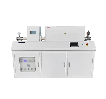
- Slide PECVD Tube Furnace with Liquid Gasifier PECVD Machine
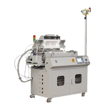
- Inclined Rotary Plasma Enhanced Chemical Deposition PECVD Tube Furnace Machine
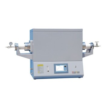
- Custom Made Versatile CVD Tube Furnace Chemical Vapor Deposition CVD Equipment Machine
- Multi Heating Zones CVD Tube Furnace Machine for Chemical Vapor Deposition Equipment
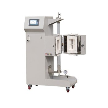
- Vertical Laboratory Quartz Tube Furnace Tubular Furnace
People Also Ask
- Why is a high vacuum diffusion pump system required when preparing Ge-Se-Te-In reaction materials? Ensure Peak Purity
- How does chemical vapour deposition (CVD) differ from PVD? Key Differences in Thin-Film Coating Methods
- What parameters control the quality of PECVD-deposited films? Master Key Variables for Superior Film Properties
- How is silicon dioxide deposited from tetraethylorthosilicate (TEOS) in PECVD? Achieve Low-Temperature, High-Quality SiO2 Films
- How does PECVD contribute to semiconductor manufacturing? Enable Low-Temperature, High-Quality Film Deposition
