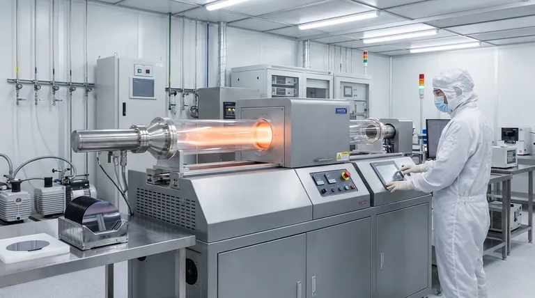
In semiconductor manufacturing, PECVD is the essential process for depositing high-quality, thin insulating films onto silicon wafers at low temperatures. It uses an energized gas, or plasma, to drive chemical reactions that would otherwise require destructive levels of heat. This allows for the construction of complex, multi-layered microchips without damaging the sensitive components already fabricated on the wafer.
The central challenge in modern chipmaking is adding new layers to a device without destroying the intricate, temperature-sensitive layers beneath. PECVD solves this by replacing brute-force heat with the targeted energy of plasma, enabling the fabrication of advanced, high-density integrated circuits.
The Core Problem: Building a Skyscraper Without Melting the Foundation
To understand the importance of PECVD, you must first appreciate the concept of a "thermal budget" in semiconductor fabrication. A chip is not built all at once; it is constructed layer by layer in a process involving hundreds of steps.
The Challenge of a Thermal Budget
Each step that involves high temperatures "spends" from the wafer's total thermal budget.
Exceeding this budget can cause previously created transistors and circuits to degrade or fail. Early fabrication steps can tolerate high heat, but later steps cannot.
Why Traditional Deposition Falls Short
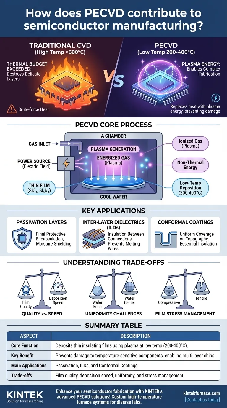
Traditional Chemical Vapor Deposition (CVD) relies on high temperatures (often >600°C) to provide the energy needed for precursor gases to react and form a solid film on the wafer.
This method is unsuitable for steps that occur after the initial transistors are formed, as this level of heat would destroy their delicate structures.
How PECVD Solves the Temperature Problem
PECVD, or Plasma-Enhanced Chemical Vapor Deposition, provides a solution by creating an entirely different energy source. It allows for deposition at much lower temperatures, typically in the 200-400°C range.
Introducing Plasma: Energy Without Extreme Heat
Instead of heat, PECVD uses an electric field to ionize gases into a state of matter called plasma.
This plasma is a highly energetic soup of ions and electrons. This energy, not thermal energy, is what breaks down the precursor gases and drives the chemical reactions needed for film deposition.
The Result: High-Quality Films on Cool Wafers
This technique allows for the deposition of dense, high-quality films like silicon dioxide (SiO₂) and silicon nitride (Si₃N₄) on wafers that remain at a relatively low temperature.
These films are critical for the function and reliability of the final device.
Key Applications Driven by Low Temperature
The low-temperature nature of PECVD makes it indispensable for several late-stage fabrication steps.
Passivation Layers: The final protective layer of silicon nitride that encapsulates a chip, shielding it from moisture and contaminants, is deposited using PECVD. Baking a completed chip at high temperatures is not an option.
Inter-Layer Dielectrics (ILDs): As minuscule copper wires are built up to connect different parts of the chip, they must be insulated from each other. PECVD deposits the dielectric (insulating) material between these wires without melting them.
Conformal Coatings: PECVD is capable of depositing films that "conform" to the topography of the chip, evenly covering the sides and bottoms of tiny trenches, which is essential for proper insulation.
Understanding the Trade-offs of PECVD
While revolutionary, PECVD is not without its complexities. The goal is always to balance speed, cost, and the specific quality metrics required for a given layer.
Film Quality vs. Deposition Speed
There is often a trade-off between the speed of deposition and the quality of the resulting film. Faster deposition can sometimes lead to films that are less dense or have more defects.
Uniformity Challenges
Achieving a perfectly uniform plasma across a large 300mm wafer is a significant engineering challenge. Non-uniformity can lead to slight variations in film thickness from the center of the wafer to the edge.
Managing Film Stress
The deposited films contain inherent mechanical stress, which can be either compressive (pushing) or tensile (pulling). Poorly managed stress can cause the wafer to bow or even crack, so controlling it is a critical parameter in any PECVD process.
Making the Right Choice for Your Process Flow
PECVD is a tool, and its application depends entirely on the specific requirements of the fabrication step.
- If your primary focus is fabricating late-stage interconnects or top-level layers: PECVD is non-negotiable, as its low temperature protects the underlying active circuitry.
- If your primary focus is creating a robust final passivation layer: PECVD is the industry standard for depositing a high-quality silicon nitride film without damaging the completed device.
- If your primary focus is on performance and precise film properties: PECVD offers exceptional control over factors like refractive index and mechanical stress, which are critical for specialized devices like MEMS and photonics.
Ultimately, PECVD is the enabling technology that allows for the vertical complexity of modern chips, making it a cornerstone of semiconductor manufacturing.
Summary Table:
| Aspect | Description |
|---|---|
| Core Function | Deposits thin insulating films (e.g., SiO₂, Si₃N₄) using plasma at low temperatures (200-400°C). |
| Key Benefit | Prevents damage to temperature-sensitive components, enabling multi-layer chip construction. |
| Main Applications | Passivation layers, inter-layer dielectrics (ILDs), and conformal coatings for insulation and protection. |
| Trade-offs | Balances film quality vs. deposition speed, uniformity challenges, and management of mechanical stress. |
Enhance your semiconductor fabrication with KINTEK's advanced PECVD solutions! Leveraging exceptional R&D and in-house manufacturing, we provide high-temperature furnace systems like CVD/PECVD tailored for diverse laboratories. Our deep customization capabilities ensure precise alignment with your unique experimental needs, from MEMS to photonics. Contact us today to discuss how our technologies can optimize your process flow and protect your sensitive components!
Visual Guide
Related Products
- RF PECVD System Radio Frequency Plasma Enhanced Chemical Vapor Deposition
- Slide PECVD Tube Furnace with Liquid Gasifier PECVD Machine
- Inclined Rotary Plasma Enhanced Chemical Deposition PECVD Tube Furnace Machine
- Inclined Rotary Plasma Enhanced Chemical Deposition PECVD Tube Furnace Machine
- Cylindrical Resonator MPCVD Machine System for Lab Diamond Growth
People Also Ask
- What is RF in PECVD? A Critical Control for Plasma Deposition
- What are the key advantages of PECVD technology? Achieve Low-Temperature, High-Quality Thin Film Deposition
- What are the advantages of PECVD in film deposition? Achieve Low-Temp, High-Quality Coatings
- How are deposition rates and film properties controlled in PECVD? Master Key Parameters for Optimal Thin Films
- What is PECVD specification? A Guide to Choosing the Right System for Your Lab


