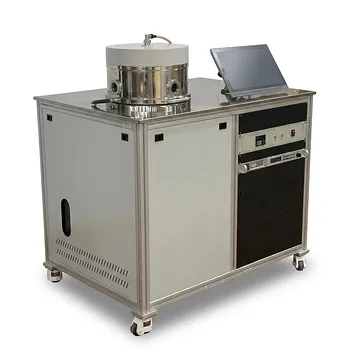
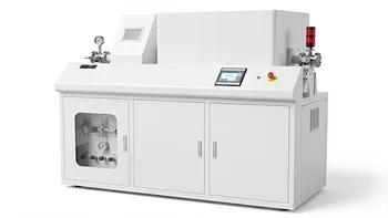
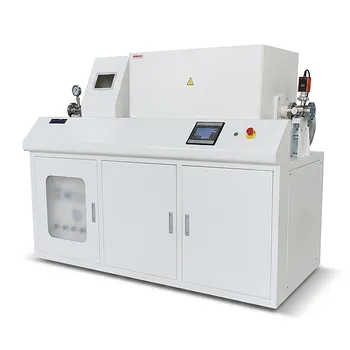
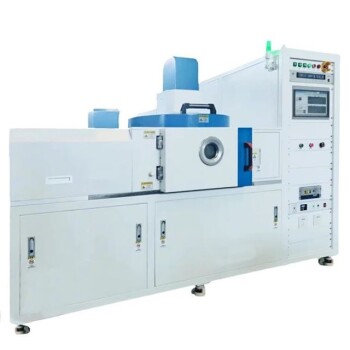
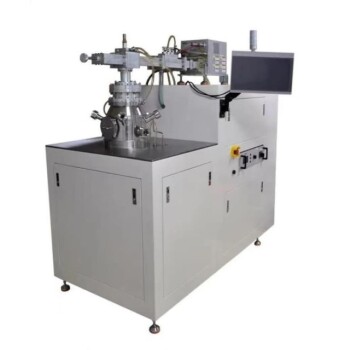
Inline Plasma Enhanced Chemical Vapor Deposition (PECVD) equipment is primarily used in solar manufacturing to deposit critical thin-film layers that passivate the silicon surface and minimize light reflection. specifically, this equipment applies Silicon Nitride (SiNx) and Aluminum Oxide (AlOx) layers, as well as doped amorphous silicon (a-Si:H) for advanced contact structures, ensuring high efficiency at mass-production scales.
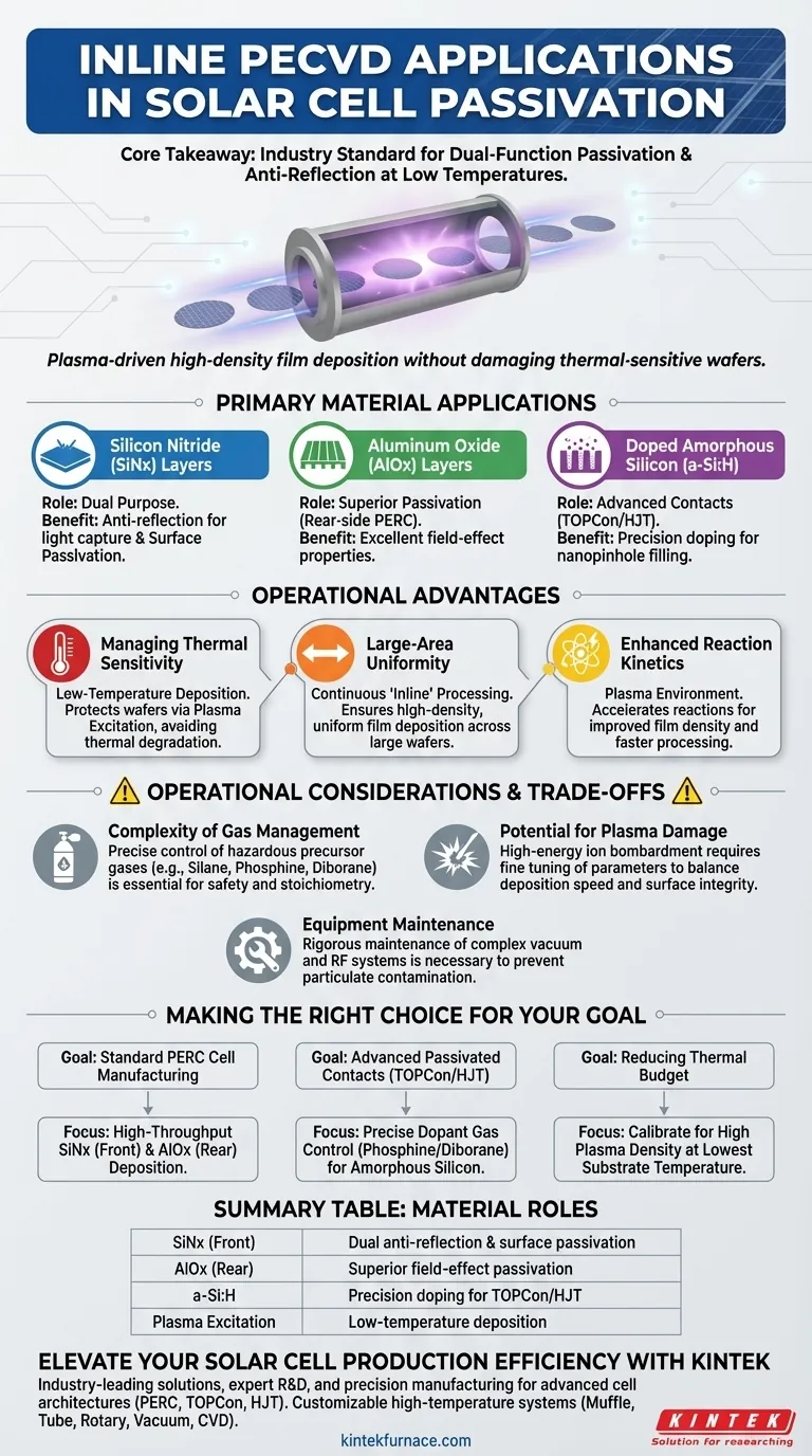
Core Takeaway Inline PECVD is the industry standard for applying multifunctional layers that simultaneously protect the solar cell electrically (passivation) and optically (anti-reflection). Its ability to drive chemical reactions via plasma rather than thermal heat allows for high-density film deposition without damaging temperature-sensitive silicon wafers.
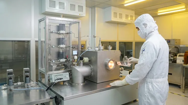
Primary Material Applications in Passivation
The primary function of inline PECVD in solar production is the deposition of specific materials that reduce electron recombination on the silicon surface.
Silicon Nitride (SiNx) Layers
This is the most common application in the industry. SiNx serves a dual purpose: it acts as an anti-reflection coating to capture more light and provides excellent surface passivation to retain electrical charge.
Aluminum Oxide (AlOx) Layers
Inline PECVD is also used to deposit Aluminum Oxide. This material provides superior passivation, particularly for the rear side of modern solar cells (such as PERC cells), due to its field-effect passivation properties.
Doped Amorphous Silicon (a-Si:H)
For advanced cell architectures, PECVD systems deposit doped amorphous silicon onto dielectric layers. By controlling gases like Phosphine or Diborane, the system ensures the material fills nanopinhole templates, creating effective passivated contacts.
The Operational Advantages of Inline PECVD
Understanding why this specific equipment is used over other deposition methods reveals the "deep need" for efficiency and quality in solar manufacturing.
Managing Thermal Sensitivity
Standard Chemical Vapor Deposition (CVD) often requires high temperatures that can degrade solar wafers. PECVD uses plasma excitation to initiate chemical reactions, allowing for the deposition of high-quality films at significantly lower temperatures.
Large-Area Uniformity
The "Inline" aspect of the equipment allows for the processing of large surface areas continuously. This system achieves high-density thin film deposition that is uniform across the entire wafer, which is critical for maintaining consistent module power output.
Enhanced Reaction Kinetics
The plasma environment creates essential electrons, ions, and neutral radicals. This accelerates reaction kinetics, leading to improved film density and faster processing times compared to non-plasma methods.
Operational Considerations and Trade-offs
While inline PECVD is highly effective, it introduces specific complexities that manufacturers must manage.
Complexity of Gas Management
The process relies on precise flows of reactive and often hazardous precursor gases, such as Silane, Phosphine, and Diborane. Safe handling and precise mass flow control are non-negotiable requirements for facility safety and film stoichiometry.
Potential for Plasma Damage
While plasma enables low-temperature processing, high-energy ion bombardment can inadvertently damage the silicon lattice surface. Process parameters must be finely tuned to balance deposition speed with surface integrity.
Equipment Maintenance
Inline vacuum systems with RF power sources are complex. They require rigorous maintenance schedules to prevent particulate contamination, which can create shunts or defects in the passivation layers.
Making the Right Choice for Your Goal
The specific configuration of PECVD equipment depends heavily on the cell architecture you are manufacturing.
- If your primary focus is standard PERC cell manufacturing: Prioritize equipment optimized for high-throughput Silicon Nitride (front) and Aluminum Oxide (rear) deposition.
- If your primary focus is advanced passivated contacts (TOPCon/HJT): Select systems with precise dopant gas control (Phosphine/Diborane) capable of filling nanopinhole structures with amorphous silicon.
- If your primary focus is reducing thermal budget: Ensure the PECVD system is calibrated for high plasma density to maximize film quality at the lowest possible substrate temperature.
Inline PECVD is not just a coating tool; it is the critical step that transforms a raw silicon wafer into a high-efficiency energy-harvesting device.
Summary Table:
| Material | Application Role | Key Benefit |
|---|---|---|
| Silicon Nitride (SiNx) | Front-side coating | Dual anti-reflection & surface passivation |
| Aluminum Oxide (AlOx) | Rear-side (PERC) | Superior field-effect passivation |
| Amorphous Silicon | Advanced contacts | Precision doping for TOPCon/HJT structures |
| Plasma Excitation | Process control | Low-temperature deposition to protect wafers |
Elevate Your Solar Cell Production Efficiency
Transitioning to advanced cell architectures like PERC, TOPCon, or HJT requires the highest standards in thin-film deposition. KINTEK provides industry-leading solutions backed by expert R&D and precision manufacturing.
Our extensive range of laboratory and industrial high-temperature systems—including Muffle, Tube, Rotary, Vacuum, and CVD systems—are fully customizable to meet your unique passivation and thermal processing needs.
Ready to optimize your solar manufacturing throughput? Contact our technical experts today to discuss how our tailored furnace and deposition solutions can enhance your material performance.
Visual Guide
References
- Pradeep Padhamnath, Armin G. Aberle. Investigation of Contact Properties and Device Performance for Bifacial Double-Side Textured Silicon Solar Cells With Polysilicon Based Passivating Contacts. DOI: 10.52825/siliconpv.v2i.1295
This article is also based on technical information from Kintek Furnace Knowledge Base .
Related Products
- Inclined Rotary Plasma Enhanced Chemical Deposition PECVD Tube Furnace Machine
- Inclined Rotary Plasma Enhanced Chemical Deposition PECVD Tube Furnace Machine
- Slide PECVD Tube Furnace with Liquid Gasifier PECVD Machine
- RF PECVD System Radio Frequency Plasma Enhanced Chemical Vapor Deposition
- Cylindrical Resonator MPCVD Machine System for Lab Diamond Growth
People Also Ask
- What are the main advantages of PECVD tube furnaces compared to CVD tube furnaces? Lower Temp, Faster Deposition, and More
- What is plasma in the context of PECVD? Unlock Low-Temperature Thin Film Deposition
- What are the typical conditions for plasma-enhanced CVD processes? Achieve Low-Temperature Thin Film Deposition
- What plasma source is used in PE-CVD tube furnaces? Unlock Low-Temperature, High-Quality Deposition
- What are some applications of rotary tube furnaces? Ideal for Continuous High-Temperature Material Processing