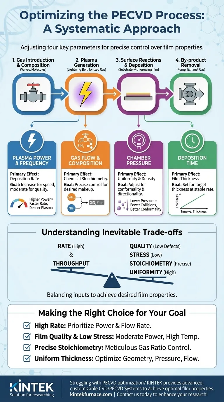
To optimize a PECVD process, you must systematically adjust four key parameters: plasma power, gas flow rates and composition, chamber pressure, and deposition time. These variables directly control the plasma's reactive species, the rate of film growth, the final film thickness, and its chemical makeup. Effective optimization is about balancing these inputs to achieve the desired film properties.
The core of PECVD optimization is not about finding one "perfect" setting, but about understanding the cause-and-effect relationship between each process parameter and the resulting film characteristics. True control comes from knowing which "knob" to turn to influence a specific outcome.
The Foundation: How PECVD Creates a Film
To optimize the process, you must first understand its fundamental steps. Each parameter you control directly influences one or more of these stages.
1. Gas Introduction & Composition
The process begins by introducing reactant gases (precursors) into the vacuum chamber. The ratio of these gases is the primary determinant of the final film's chemical composition, or stoichiometry.
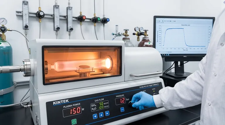
For example, when depositing silicon nitride (SiNx), the ratio of silane (SiH4) to a nitrogen source like ammonia (NH3) or nitrous oxide (N2O) directly controls the silicon-to-nitrogen ratio in the deposited film.
2. Plasma Generation
A high-frequency electric field is applied to the gas, ionizing it and creating a plasma. The plasma is a highly reactive soup of ions, electrons, and neutral radical species.
Plasma power is the key variable here. Increasing the power increases the plasma density, which creates a higher concentration of reactive species. This generally leads to a faster deposition rate.
3. Surface Reactions & Deposition
The reactive species from the plasma diffuse to the substrate surface. There, they adsorb, react, and bond to form a solid thin film.
The substrate temperature (though not directly part of plasma generation) is critical at this stage. Higher temperatures provide more energy for surface reactions and allow deposited atoms to move around (surface mobility), often resulting in a denser, higher-quality film with less internal stress.
4. By-product Removal
Gaseous by-products from the surface reactions must be continuously pumped out of the chamber. Chamber pressure and gas flow rates are critical for this.
Lowering the pressure increases the mean free path of particles and can make ions more directional, while the total gas flow rate influences the residence time of reactive species in the chamber.
Key Optimization Parameters and Their Effects
Think of optimization as a multi-variable equation. Changing one parameter often has cascading effects on the others and the final film.
Plasma Power & Frequency
This is your primary control for deposition rate. Higher power creates a denser plasma, generating more film-forming radicals and ions. The frequency of the electric field (e.g., RF or microwave) also influences the plasma's characteristics and the energy of ions bombarding the substrate.
Gas Flow and Composition
This directly controls the film's chemical makeup. To create a specific material like silicon dioxide (SiO2) or silicon nitride (SiNx), you must supply the constituent elements in a precise, stable ratio.
Chamber Pressure
Pressure influences the uniformity and density of the film. Lower pressures lead to fewer gas-phase collisions, allowing reactive species to travel in straighter lines to the substrate. This can improve conformality (how well the film covers steps) and directionality.
Deposition Time
This is the simplest variable. For a given stable set of process conditions, film thickness is directly proportional to the deposition time. Once your rate is established and stable, you use time to achieve your target thickness.
Understanding the Inevitable Trade-offs
Optimizing for one property often comes at the expense of another. Recognizing these trade-offs is the mark of an expert.
Rate vs. Quality
Pushing for a very high deposition rate by increasing plasma power or gas flow can be detrimental. It can lead to more defects, higher hydrogen incorporation (which can affect electronic properties), and increased internal film stress.
Stress vs. Stoichiometry
Achieving the perfect chemical ratio (stoichiometry) can sometimes result in a film with high internal stress. This stress can cause the film to crack or delaminate from the substrate. Fine-tuning other parameters like temperature or ion bombardment (via power/pressure) is often required to mitigate this.
Uniformity vs. Throughput
High gas flow rates can increase throughput but may lead to non-uniform deposition across a large substrate. The center of the wafer might see a different gas concentration than the edge, resulting in variations in thickness or composition.
Making the Right Choice for Your Goal
Your optimization strategy depends entirely on what film characteristic is most important for your application.
- If your primary focus is a high deposition rate: Prioritize increasing plasma power and the total flow rate of your reactant gases.
- If your primary focus is film quality and low stress: Use moderate plasma power and a relatively high substrate temperature to enhance surface mobility and promote a dense microstructure.
- If your primary focus is precise stoichiometry: Meticulously control and stabilize the flow rate ratio of your precursor gases, using characterization tools to verify the film's composition.
- If your primary focus is uniform thickness across the wafer: Focus on optimizing the chamber geometry, pressure, and gas flow dynamics to ensure even distribution of reactive species.
Ultimately, PECVD optimization is a systematic process of balancing these interconnected variables to achieve a specific engineering outcome.
Summary Table:
| Parameter | Primary Effect on Film | Key Optimization Goal |
|---|---|---|
| Plasma Power | Deposition Rate | Increase for speed, moderate for quality |
| Gas Flow & Composition | Chemical Stoichiometry | Precise control for desired film makeup |
| Chamber Pressure | Uniformity & Density | Adjust for conformality and directionality |
| Deposition Time | Film Thickness | Set for target thickness at stable rate |
| Substrate Temperature | Film Quality & Stress | Higher for denser, lower-stress films |
Struggling with PECVD optimization for your lab's thin-film processes? KINTEK leverages exceptional R&D and in-house manufacturing to provide advanced high-temperature furnace solutions, including CVD/PECVD Systems. Our strong deep customization capability ensures precise alignment with your unique experimental needs, helping you achieve optimal film properties and efficiency. Contact us today to discuss how our tailored solutions can enhance your research and production outcomes!
Visual Guide
Related Products
- RF PECVD System Radio Frequency Plasma Enhanced Chemical Vapor Deposition
- Slide PECVD Tube Furnace with Liquid Gasifier PECVD Machine
- Inclined Rotary Plasma Enhanced Chemical Deposition PECVD Tube Furnace Machine
- Inclined Rotary Plasma Enhanced Chemical Deposition PECVD Tube Furnace Machine
- Cylindrical Resonator MPCVD Machine System for Lab Diamond Growth
People Also Ask
- What are the advantages of PECVD in film deposition? Achieve Low-Temp, High-Quality Coatings
- How are deposition rates and film properties controlled in PECVD? Master Key Parameters for Optimal Thin Films
- How is silicon dioxide deposited from tetraethylorthosilicate (TEOS) in PECVD? Achieve Low-Temperature, High-Quality SiO2 Films
- How does film quality compare between PECVD and CVD? Choose the Best Method for Your Substrate
- What are the applications of plasma enhanced chemical vapor deposition? Key Uses in Electronics, Optics & Materials


