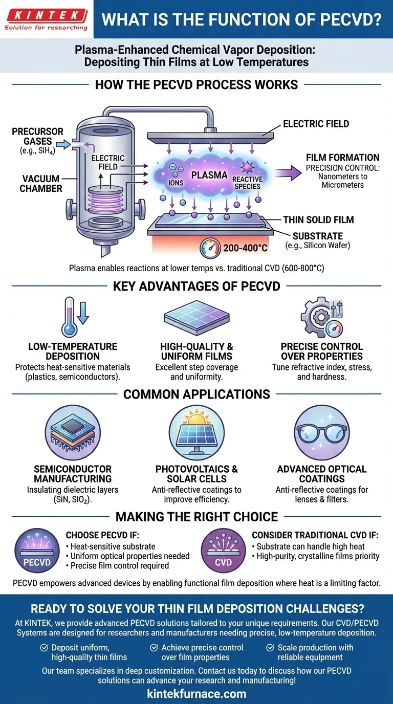
The primary function of Plasma-Enhanced Chemical Vapor Deposition (PECVD) is to deposit thin, solid films onto a substrate from a gas state. It is a specialized manufacturing process that uses an energized plasma to enable these chemical reactions to occur at significantly lower temperatures than traditional methods, making it ideal for heat-sensitive materials.
PECVD solves a critical manufacturing challenge: how to deposit high-quality, uniform thin films onto materials that cannot withstand high heat. Its function is not just to create a coating, but to do so with precise control and without damaging the underlying substrate.
How the PECVD Process Works
PECVD is fundamentally a chemical deposition process that gets a major boost from plasma physics. Understanding the role of the plasma is key to understanding the function of the entire system.
The Role of Plasma
The "plasma-enhanced" part of the name is the critical innovation. In a vacuum chamber, an electric field is used to energize precursor gases, such as silane (SiH4).
This energy doesn't burn the gas; instead, it strips electrons from the gas molecules, creating a highly reactive state of matter known as plasma.
This plasma contains ions and other reactive species that can form a solid film at much lower temperatures (e.g., 200-400°C) compared to traditional Chemical Vapor Deposition (CVD), which might require over 600-800°C.
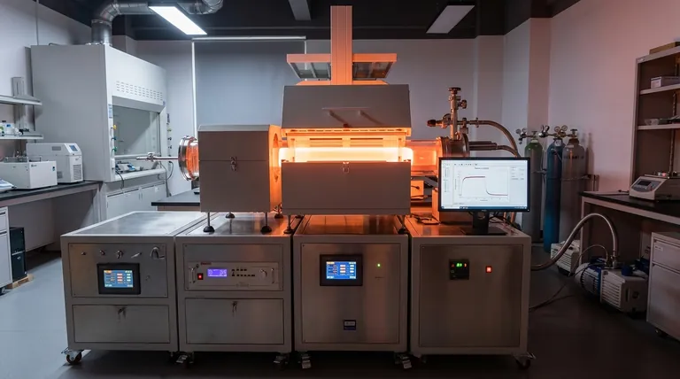
The Deposition Chamber
The entire process occurs inside a highly controlled vacuum chamber. Precursor gases are introduced at very low pressures.
Electrodes within the chamber generate the electric field that ignites and sustains the plasma.
The substrate, often a silicon wafer or piece of glass, is placed on a holder that can be heated to a precise, controlled temperature, ensuring the film adheres correctly and has the desired properties.
Film Formation
Once the plasma is active, the reactive gas species move throughout the chamber and land on the substrate's surface.
These reactive components then bond to the surface and to each other, gradually building up a solid, uniform thin film.
The thickness of this film can be precisely controlled, from just a few nanometers to several micrometers, by adjusting the process time, gas flow, and plasma power.
Key Advantages of the PECVD Process
The unique low-temperature, plasma-driven nature of PECVD provides several distinct advantages that make it the preferred choice for specific, high-value applications.
Low-Temperature Deposition
This is the most significant advantage. It allows for the coating of materials, like certain semiconductors or plastics, that would be damaged or destroyed by the high temperatures of other deposition methods.
High-Quality and Uniform Films
PECVD is renowned for producing films with excellent uniformity across the entire surface of the substrate.
It also provides good step coverage, meaning the film conforms evenly over non-flat surfaces and microscopic features on a semiconductor chip.
Precise Control Over Film Properties
By carefully adjusting process parameters like gas composition, pressure, temperature, and plasma density, engineers can fine-tune the material properties of the film.
This includes critical characteristics like refractive index (for optics), internal stress, and hardness, allowing for the creation of highly specialized materials.
Common Applications
The combination of low-temperature processing and high-quality results makes PECVD essential in several advanced manufacturing sectors.
Semiconductor Manufacturing
In producing integrated circuits, PECVD is used to deposit insulating layers (dielectrics) like silicon nitride (SiN) or silicon dioxide (SiO2). These layers isolate different conductive parts of the microchip from one another.
Photovoltaics and Solar Cells
PECVD is crucial for manufacturing thin-film solar cells. It is used to deposit layers like amorphous silicon and anti-reflective coatings of silicon nitride.
These coatings improve the efficiency of the solar cell by maximizing the amount of light it can absorb.
Advanced Optical Coatings
The process is used to create highly specific optical coatings. This includes anti-reflective coatings on eyeglass lenses and camera optics, as well as specialized filters.
By controlling the refractive index, PECVD can create coatings that reduce glare and improve the performance and durability of optical products.
Making the Right Choice for Your Application
Choosing a deposition technology depends entirely on your material constraints and desired film properties.
- If your primary focus is depositing on a heat-sensitive substrate: PECVD is the definitive choice because its low-temperature process prevents damage.
- If your primary focus is creating a uniform film with specific optical properties: PECVD offers the precise control over refractive index and thickness needed for advanced optical coatings.
- If your primary focus is creating high-purity, crystalline films and your substrate can handle heat: You might consider traditional high-temperature CVD, as it can sometimes yield higher purity for certain materials.
Ultimately, PECVD empowers the creation of advanced devices by enabling the deposition of functional films where heat is a limiting factor.
Summary Table:
| Key Feature | Benefit |
|---|---|
| Low-Temperature Deposition | Protects heat-sensitive substrates like plastics and advanced semiconductors |
| Plasma-Enhanced Reactions | Enables film formation at 200-400°C vs. 600-800°C in traditional CVD |
| Uniform Film Quality | Provides excellent step coverage and thickness control across complex surfaces |
| Precise Property Control | Allows tuning of refractive index, stress, and hardness for specific applications |
| Versatile Applications | Essential for semiconductors, solar cells, and advanced optical coatings |
Ready to solve your thin film deposition challenges?
At KINTEK, we leverage our exceptional R&D and in-house manufacturing capabilities to provide advanced PECVD solutions tailored to your unique requirements. Our CVD/PECVD Systems are designed for researchers and manufacturers who need precise, low-temperature deposition for heat-sensitive materials.
We help you:
- Deposit uniform, high-quality thin films without damaging temperature-sensitive substrates
- Achieve precise control over film properties like refractive index and stress
- Scale your semiconductor, photovoltaic, or optical coating production with reliable equipment
Our team specializes in deep customization to ensure your PECVD system perfectly matches your experimental or production needs.
Contact us today to discuss how our PECVD solutions can advance your research and manufacturing!
Visual Guide
Related Products
- Slide PECVD Tube Furnace with Liquid Gasifier PECVD Machine
- RF PECVD System Radio Frequency Plasma Enhanced Chemical Vapor Deposition
- Inclined Rotary Plasma Enhanced Chemical Deposition PECVD Tube Furnace Machine
- Inclined Rotary Plasma Enhanced Chemical Deposition PECVD Tube Furnace Machine
- Multi Heating Zones CVD Tube Furnace Machine for Chemical Vapor Deposition Equipment
People Also Ask
- What are the main advantages of PECVD tube furnaces compared to CVD tube furnaces? Lower Temp, Faster Deposition, and More
- What plasma source is used in PE-CVD tube furnaces? Unlock Low-Temperature, High-Quality Deposition
- What are the typical conditions for plasma-enhanced CVD processes? Achieve Low-Temperature Thin Film Deposition
- In which industries is the tube furnace commonly used? Essential for Materials Science, Energy, and More
- What is plasma in the context of PECVD? Unlock Low-Temperature Thin Film Deposition


