In short, Plasma-Enhanced Chemical Vapor Deposition (PECVD) is primarily used to deposit dielectric films like silicon dioxide and silicon nitride, as well as various forms of silicon, including amorphous and polycrystalline silicon. The process is also capable of depositing certain compound semiconductor, epitaxial, and metallic thin films where low processing temperatures are a critical requirement.
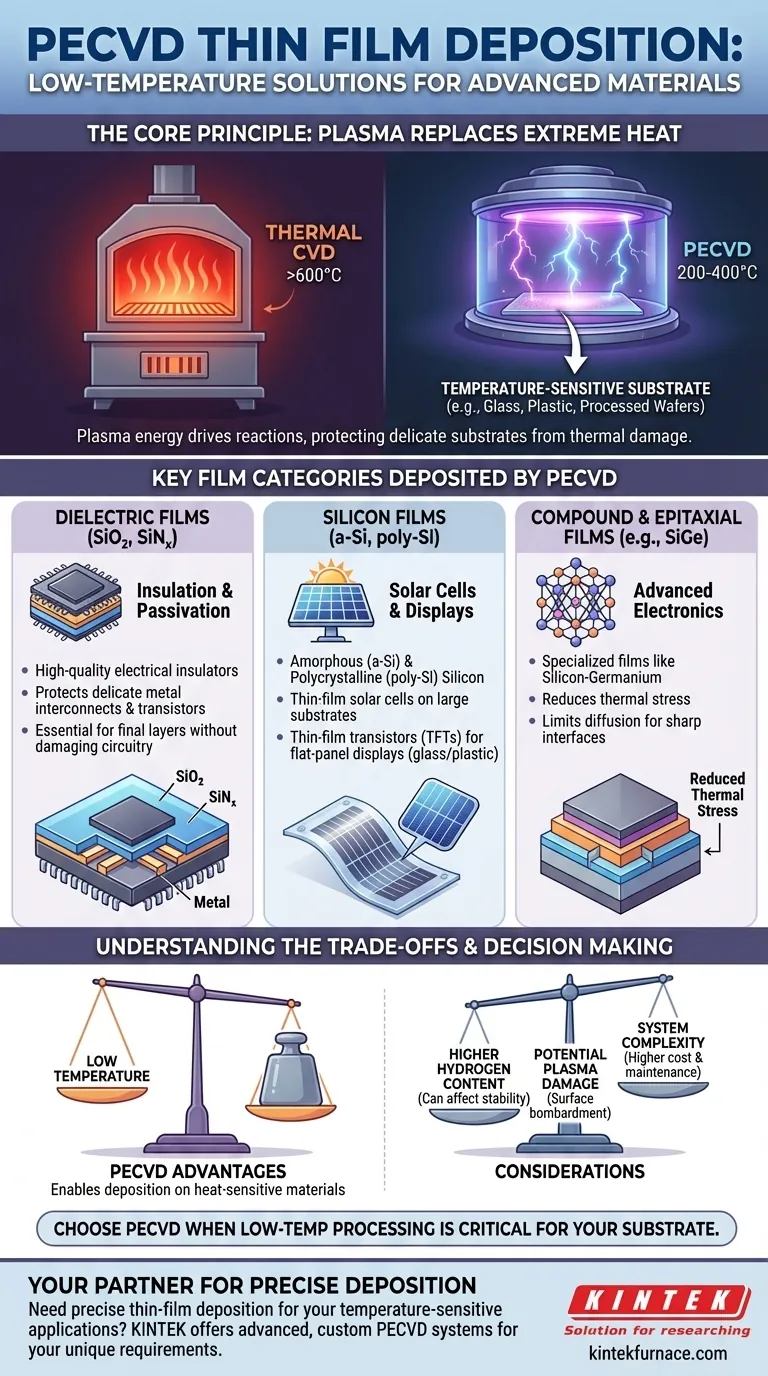
The defining characteristic of PECVD is not the specific materials it can deposit, but its ability to do so at significantly lower temperatures than conventional methods. This single advantage makes it the go-to process for depositing high-quality films onto substrates that cannot withstand thermal damage.
The Core Principle of PECVD: Deposition Without Extreme Heat
To understand why certain films are associated with PECVD, you must first grasp its fundamental advantage over traditional Chemical Vapor Deposition (CVD).
How Plasma Replaces Heat
In conventional CVD, high temperatures (often >600°C) are required to provide the energy needed to break down precursor gases and initiate the chemical reaction that forms the film on a substrate.
PECVD replaces this intense thermal energy with energy from a plasma. By applying a radio frequency (RF) or microwave field to a low-pressure gas, it creates highly reactive ions and radicals that can drive the deposition reaction at much lower temperatures, typically in the 200-400°C range.
The Impact on Material Choice
This low-temperature capability is not just an incremental improvement; it is a transformative one. It opens up the possibility of depositing films on substrates that would be warped, melted, or otherwise destroyed by high-temperature processes. This is the central reason behind PECVD's specific applications.
Key Film Categories Deposited by PECVD
While the list of potential films is long, the most common applications are driven by the need to protect temperature-sensitive structures.
Dielectric Films (SiO₂, SiNₓ)
This is the most widespread use of PECVD in the semiconductor industry. Films like silicon dioxide (SiO₂) and silicon nitride (SiNₓ) are deposited as high-quality electrical insulators and protective layers.
Because these films are often applied late in the manufacturing process, the underlying wafer already contains delicate metal interconnects and transistors. The low temperature of PECVD is essential for depositing these final passivation or insulating layers without damaging the completed circuitry.
Silicon Films (a-Si, poly-Si)
PECVD is critical for depositing amorphous silicon (a-Si) and polycrystalline silicon (poly-Si). These materials are foundational for two major industries.
First, in photovoltaics, a-Si is used to create thin-film solar cells on large, inexpensive substrates like glass. Second, in flat-panel displays, these silicon films form the thin-film transistors (TFTs) that control the pixels on glass or even flexible plastic substrates. High-temperature deposition is simply not an option for these applications.
Compound and Epitaxial Films
While less common, PECVD can be used for growing specialized films like silicon-germanium (SiGe) or certain compound semiconductors.
Here, the low-temperature advantage helps reduce thermal stress between the film and the substrate and limits unwanted diffusion of atoms between layers, which is critical for creating sharp interfaces in advanced electronic devices.
Understanding the Trade-offs
PECVD is a powerful tool, but it is not without its compromises. Choosing it means accepting certain trade-offs compared to higher-temperature methods.
Film Quality and Hydrogen Content
Because the precursor gases are broken down by plasma instead of heat, PECVD films often have a significant amount of hydrogen incorporated into them. This can be beneficial in some cases (passivating defects) but detrimental in others, where it can affect the film's electrical stability and performance. High-temperature CVD typically produces purer films with lower hydrogen content.
Potential for Plasma-Induced Damage
The high-energy ions within the plasma can physically bombard the substrate surface during deposition. While this can sometimes improve film density, it also carries the risk of creating surface damage, which can be problematic for highly sensitive electronic devices.
System Complexity
PECVD reactors are more complex and expensive than their thermal CVD counterparts. They require sophisticated RF power generation and delivery systems, impedance matching networks, and robust vacuum controls to sustain and manage the plasma.
Making the Right Choice for Your Application
Selecting a deposition method depends entirely on the constraints of your substrate and the required properties of your film.
- If your primary focus is protecting underlying structures: PECVD is the industry standard for depositing dielectric insulation and passivation layers on fully fabricated wafers or other temperature-sensitive components.
- If your primary focus is deposition on large-area or low-temperature substrates: PECVD is essential for applications like thin-film solar cells or displays on glass and plastic.
- If your primary focus is the absolute highest crystal quality and purity: You may need to consider higher-temperature methods like thermal CVD or Molecular Beam Epitaxy (MBE), especially if hydrogen content is a concern.
Ultimately, understanding PECVD's low-temperature advantage is the key to leveraging its power for advanced material deposition.
Summary Table:
| Film Type | Common Materials | Key Applications |
|---|---|---|
| Dielectric | Silicon Dioxide (SiO₂), Silicon Nitride (SiNₓ) | Electrical insulation, passivation in semiconductors |
| Silicon | Amorphous Silicon (a-Si), Polycrystalline Silicon (poly-Si) | Thin-film solar cells, flat-panel displays |
| Compound/Epitaxial | Silicon-Germanium (SiGe) | Advanced electronics with reduced thermal stress |
Need precise thin-film deposition for your temperature-sensitive applications? KINTEK leverages exceptional R&D and in-house manufacturing to provide advanced PECVD systems and other high-temperature furnace solutions like Muffle, Tube, Rotary, Vacuum & Atmosphere Furnaces, and CVD/PECVD Systems. Our strong deep customization capability ensures we meet your unique experimental requirements—contact us today to enhance your lab's efficiency and innovation!
Visual Guide
Related Products
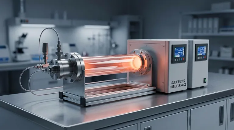
- RF PECVD System Radio Frequency Plasma Enhanced Chemical Vapor Deposition
- Slide PECVD Tube Furnace with Liquid Gasifier PECVD Machine
- Inclined Rotary Plasma Enhanced Chemical Deposition PECVD Tube Furnace Machine
- Inclined Rotary Plasma Enhanced Chemical Deposition PECVD Tube Furnace Machine
People Also Ask
- What are some promising applications of PECVD-prepared 2D materials? Unlock Advanced Sensing and Optoelectronics
- How is silicon dioxide deposited from tetraethylorthosilicate (TEOS) in PECVD? Achieve Low-Temperature, High-Quality SiO2 Films
- What is the role of RF power in PECVD and how does the RF-PECVD process work? Master Thin Film Deposition Control
- What is RF in PECVD? A Critical Control for Plasma Deposition
- How are deposition rates and film properties controlled in PECVD? Master Key Parameters for Optimal Thin Films


