The primary reason for utilizing a Plasma Enhanced Chemical Vapor Deposition (PECVD) system in monolithic integrated chips is its ability to deposit high-quality silicon dioxide (SiO2) thin films at relatively low temperatures. While traditional deposition methods often require high heat that can damage sensitive components, PECVD uses plasma energy to drive the necessary chemical reactions, ensuring the integrity of the underlying device structure.
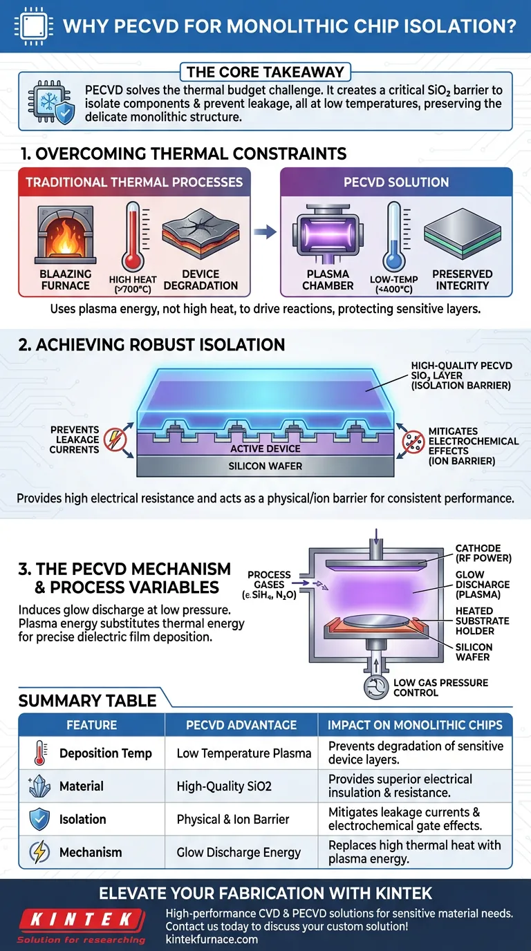
Core Takeaway: PECVD solves the thermal budget challenge in chip manufacturing. It creates a critical silicon dioxide barrier that electrically isolates components and prevents leakage currents, all without exposing the delicate monolithic structure to destructive high-temperature processes.
The Critical Role of Temperature Control
Overcoming Thermal Constraints
In monolithic integration, preserving the stability of existing layers is paramount. Traditional thermal processes often require temperatures that could degrade the device.
PECVD circumvents this by utilizing a low-temperature plasma within the process chamber. This allows for the formation of solid films without subjecting the substrate to the intense heat usually required to trigger chemical bonding.
The Mechanism of Action
The system operates by inducing a glow discharge at the cathode under low gas pressure. Once process gases are introduced, they undergo specific plasma and chemical reactions.
This energy substitution—using plasma rather than pure thermal energy—enables the precise deposition of dielectric films on silicon wafers while keeping the environment relatively cool.
Achieving Robust Isolation
Eliminating Electrical Leakage
The primary function of the SiO2 layer produced by PECVD is to act as an electrical isolation barrier.
The deposited film provides high electrical resistance. This is essential for preventing leakage currents that would otherwise compromise the efficiency and functionality of the integrated chip.
Mitigating Electrochemical Effects
Beyond simple electrical insulation, the layer functions as a crucial physical and ion barrier.
This barrier serves to mitigate electrochemical gate effects. By physically separating components, the SiO2 layer prevents external factors from disrupting the semiconductor carrier distribution, ensuring consistent device performance.
Understanding the Process Variables
Complexity of Deposition Parameters
While PECVD offers thermal advantages, it introduces process complexity regarding gas regulation. The quality of the film relies heavily on maintaining a specific low gas pressure environment.
Operators must carefully control the introduction of process gases after the sample reaches its specific (lower) target temperature. Deviations in pressure or gas flow can alter the chemical reactions, potentially affecting the uniformity or density of the isolation layer.
Making the Right Choice for Your Goal
To determine if PECVD is the correct solution for your specific integration needs, consider your primary constraints:
- If your primary focus is preserving temperature-sensitive layers: PECVD is the optimal choice, as it deposits essential dielectric films without exceeding the thermal budget of the substrate.
- If your primary focus is preventing signal cross-talk and leakage: Reliance on the high-quality SiO2 films from PECVD provides the high resistance necessary to eliminate leakage currents.
- If your primary focus is stabilizing carrier distribution: The physical barrier properties of PECVD films are required to mitigate electrochemical gate effects and shield against ion movement.
By leveraging plasma energy to replace thermal intensity, PECVD allows for the creation of robust, isolated monolithic structures that would otherwise be impossible to manufacture.
Summary Table:
| Feature | PECVD Advantage | Impact on Monolithic Chips |
|---|---|---|
| Deposition Temp | Low Temperature Plasma | Prevents degradation of sensitive device layers. |
| Material | High-Quality SiO2 | Provides superior electrical insulation and resistance. |
| Isolation | Physical & Ion Barrier | Mitigates leakage currents and electrochemical gate effects. |
| Mechanism | Glow Discharge Energy | Replaces high thermal heat with plasma energy. |
Elevate Your Semiconductor Fabrication with KINTEK
Precision matters when your monolithic structures are on the line. Backed by expert R&D and manufacturing, KINTEK offers high-performance CVD systems, PECVD solutions, and customizable lab high-temp furnaces designed specifically for sensitive material needs.
Whether you are looking to optimize your thermal budget or enhance dielectric isolation, our team is ready to provide the specialized equipment your unique project demands.
Ready to upgrade your laboratory capabilities? Contact us today to discuss your custom solution!
Visual Guide
References
- Sixing Xu, Xiaohong Wang. Wafer-level heterogeneous integration of electrochemical devices and semiconductors for a monolithic chip. DOI: 10.1093/nsr/nwae049
This article is also based on technical information from Kintek Furnace Knowledge Base .
Related Products
- RF PECVD System Radio Frequency Plasma Enhanced Chemical Vapor Deposition
- Slide PECVD Tube Furnace with Liquid Gasifier PECVD Machine
- Inclined Rotary Plasma Enhanced Chemical Deposition PECVD Tube Furnace Machine
- Inclined Rotary Plasma Enhanced Chemical Deposition PECVD Tube Furnace Machine
- 915MHz MPCVD Diamond Machine Microwave Plasma Chemical Vapor Deposition System Reactor
People Also Ask
- What is RF in PECVD? A Critical Control for Plasma Deposition
- How are deposition rates and film properties controlled in PECVD? Master Key Parameters for Optimal Thin Films
- What is PECVD specification? A Guide to Choosing the Right System for Your Lab
- What are some promising applications of PECVD-prepared 2D materials? Unlock Advanced Sensing and Optoelectronics
- What are the advantages of PECVD in film deposition? Achieve Low-Temp, High-Quality Coatings


