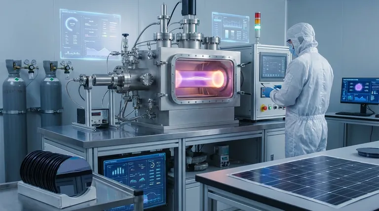
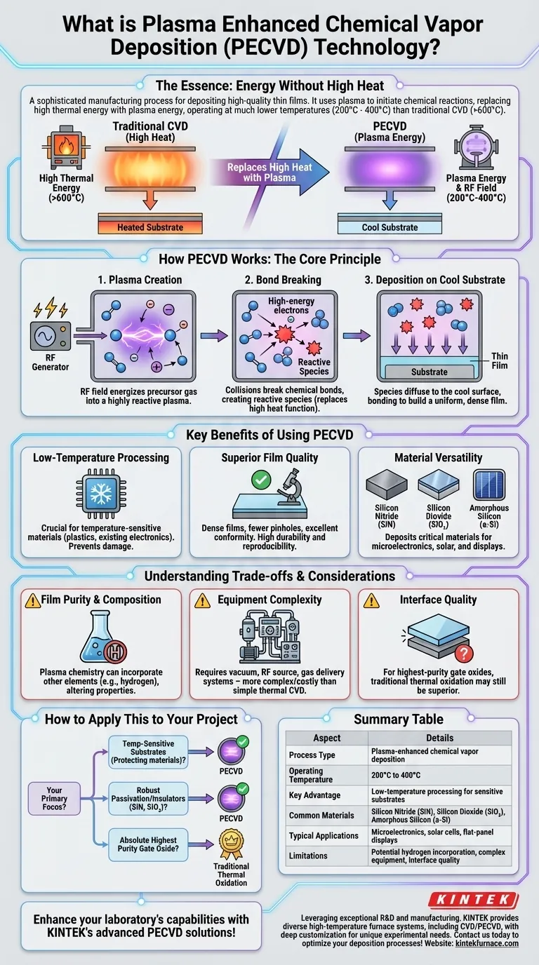
In essence, Plasma Enhanced Chemical Vapor Deposition (PECVD) is a sophisticated manufacturing process used to deposit high-quality thin films onto a surface. It is a variation of Chemical Vapor Deposition (CVD) that uniquely uses plasma to initiate chemical reactions. This critical difference allows the process to operate at much lower temperatures than traditional CVD, making it indispensable for modern electronics and material science.
The central advantage of PECVD is its ability to replace high heat with plasma energy. This allows for the creation of durable, high-performance thin films on temperature-sensitive materials that would be damaged or destroyed by conventional high-temperature deposition methods.
The Core Principle: How PECVD Works
To understand PECVD, it is useful to first consider the limitations of its predecessor, traditional thermal CVD.
The Limitation of Traditional CVD
Traditional Chemical Vapor Deposition is like a conventional oven. It relies purely on high thermal energy (often >600°C) to break down precursor gases and deposit a solid film onto a heated substrate.
While effective, this intense heat makes it unsuitable for substrates that have already been processed or are inherently sensitive to temperature, such as plastics or certain electronic components.
The Plasma Advantage: Energy Without Heat
PECVD circumvents the need for extreme heat by introducing an energy source: plasma. A plasma is a state of matter, an ionized gas containing a mix of ions, electrons, and neutral particles.
Inside the PECVD chamber, an electric field (typically Radio Frequency, or RF) energizes a gas, turning it into a plasma. The highly energetic electrons within this plasma collide with the precursor gas molecules.
These collisions have enough energy to break the chemical bonds of the precursor gases, creating highly reactive species. This is the key step that high heat performs in traditional CVD.
The Deposition Process
Once these reactive species are created in the plasma, they diffuse toward the comparatively cool substrate.
Upon reaching the surface, they react and bond, gradually building up a solid, uniform, and dense thin film. The entire process can occur at much lower temperatures, typically between 200°C and 400°C.
Key Benefits of Using PECVD
The unique mechanism of PECVD provides several distinct advantages that have made it a cornerstone technology in multiple industries.
Low-Temperature Processing
This is the primary benefit. The ability to deposit films at low temperatures enables the fabrication of complex, multi-layered devices without damaging previously deposited layers or the underlying substrate.
Superior Film Quality
PECVD films are known for being very dense, with fewer pinholes and excellent surface conformity. This results in greater durability and better performance as protective or insulating layers. It is a reliable and highly reproducible process.
Material Versatility
The process is used to deposit a wide range of critical materials. Common examples include:
- Silicon Nitride (SiN): Used as a final passivation layer in microchips to protect against moisture and contamination.
- Silicon Dioxide (SiO₂): Used as an insulator between metal layers in integrated circuits.
- Amorphous Silicon (a-Si): A key material used in the manufacturing of thin-film solar cells and flat-panel displays.
Understanding the Trade-offs and Considerations
While powerful, PECVD is not a universal solution. Understanding its limitations is crucial for making informed engineering decisions.
Film Purity and Composition
The complex chemistry within the plasma can sometimes lead to the incorporation of other elements, such as hydrogen, into the deposited film. This can alter the film's electrical or optical properties, which may be undesirable for certain high-purity applications.
Equipment Complexity
A PECVD system requires a vacuum chamber, a gas delivery system, and an RF power source to generate the plasma. This makes the equipment more complex and costly than some simpler thermal CVD setups.
Interface Quality
For the most demanding applications, like the gate oxide in a transistor, a film grown with high-temperature thermal oxidation often creates a higher-quality electrical interface with the silicon substrate than a deposited PECVD film.
How to Apply This to Your Project
Your choice of deposition technology depends entirely on your project's constraints and desired outcome.
- If your primary focus is depositing on temperature-sensitive substrates: PECVD is the definitive choice due to its low-temperature operation, protecting underlying materials and components.
- If your primary focus is creating robust passivation layers or dielectric insulators: PECVD provides a reliable, industry-standard method for depositing high-density films like silicon nitride and silicon dioxide.
- If your primary focus is achieving the absolute highest purity for a gate oxide: Traditional high-temperature thermal oxidation on a silicon wafer remains the gold standard for that specific application.
By understanding the interplay between plasma energy and thermal budget, you can strategically leverage PECVD to achieve high-performance thin films where other methods would fail.
Summary Table:
| Aspect | Details |
|---|---|
| Process Type | Plasma-enhanced chemical vapor deposition |
| Operating Temperature | 200°C to 400°C |
| Key Advantage | Low-temperature processing for sensitive substrates |
| Common Materials Deposited | Silicon Nitride (SiN), Silicon Dioxide (SiO₂), Amorphous Silicon (a-Si) |
| Typical Applications | Microelectronics, solar cells, flat-panel displays |
| Limitations | Potential for hydrogen incorporation, equipment complexity, interface quality concerns |
Enhance your laboratory's capabilities with KINTEK's advanced PECVD solutions! Leveraging exceptional R&D and in-house manufacturing, we provide diverse labs with high-temperature furnace systems like CVD/PECVD, Muffle, Tube, Rotary, and Vacuum & Atmosphere Furnaces. Our deep customization ensures precise alignment with your unique experimental needs, delivering durable thin films for electronics and material science. Contact us today to discuss how we can optimize your deposition processes and boost performance!
Visual Guide
Related Products
- RF PECVD System Radio Frequency Plasma Enhanced Chemical Vapor Deposition
- Slide PECVD Tube Furnace with Liquid Gasifier PECVD Machine
- Inclined Rotary Plasma Enhanced Chemical Deposition PECVD Tube Furnace Machine
- Inclined Rotary Plasma Enhanced Chemical Deposition PECVD Tube Furnace Machine
- 915MHz MPCVD Diamond Machine Microwave Plasma Chemical Vapor Deposition System Reactor
People Also Ask
- What are the key advantages of PECVD technology? Achieve Low-Temperature, High-Quality Thin Film Deposition
- How is silicon dioxide deposited from tetraethylorthosilicate (TEOS) in PECVD? Achieve Low-Temperature, High-Quality SiO2 Films
- How are deposition rates and film properties controlled in PECVD? Master Key Parameters for Optimal Thin Films
- What is the role of RF power in PECVD and how does the RF-PECVD process work? Master Thin Film Deposition Control
- What is PECVD specification? A Guide to Choosing the Right System for Your Lab


