The fundamental advantage of low-temperature Plasma-Enhanced Chemical Vapor Deposition (PECVD) is its ability to grow high-quality thin films without the damaging high temperatures required by conventional methods. This process uses plasma to energize precursor gases, allowing chemical reactions and deposition to occur at significantly lower temperatures. This core capability enables the coating of delicate, temperature-sensitive materials while improving film quality and operational efficiency.
The critical takeaway is that low-temperature PECVD replaces brute-force thermal energy with targeted plasma energy. This decoupling of reaction activation from heat is what allows it to deposit robust films on materials, from flexible polymers to complex microchips, that would be destroyed by traditional deposition processes.
The Core Principle: Plasma as a Substitute for Heat
To fully grasp the advantages of low-temperature PECVD, you must first understand how it differs from its conventional thermal counterpart. The key is how the chemical precursors are activated.
How Traditional CVD Works
Conventional Chemical Vapor Deposition (CVD) relies entirely on thermal energy. Substrates are heated to very high temperatures (often >600°C) to provide enough energy to break the chemical bonds of the precursor gases, allowing them to react and deposit as a thin film.
This high-heat requirement is a major limitation. It restricts the process to only those substrates that can withstand extreme thermal stress without melting, warping, or degrading.
How PECVD Bypasses the Heat Requirement
PECVD ingeniously circumvents the need for high heat by introducing plasma. An electric field (typically radio frequency) is applied to the precursor gases, stripping electrons from their atoms and creating an ionized gas, or plasma.
The free electrons in the plasma are highly energetic. When they collide with the precursor gas molecules, they transfer their energy and break the chemical bonds. This creates highly reactive radicals that can then deposit on a nearby substrate, which can be kept at a much lower temperature (e.g., <400°C).
Key Advantages Explained
This plasma-driven mechanism unlocks several significant advantages that have made low-temperature PECVD a cornerstone of modern manufacturing.
Preserving Substrate Integrity
The most cited advantage is the ability to deposit films on temperature-sensitive substrates. By lowering process temperatures, PECVD minimizes thermal stress and prevents damage.
This capability is critical for applications involving plastics, polymers, or fully fabricated semiconductor devices where additional high-temperature steps would destroy the existing integrated circuits.
Achieving Superior Film Quality
While it operates at lower temperatures, PECVD often produces films with excellent characteristics. The energetic plasma environment can lead to the formation of dense films with fewer pinholes and a lower likelihood of cracking.
This results in uniform, high-purity layers with good adhesion, which are essential for creating reliable protective barriers, dielectric insulators, and optical coatings.
Unlocking Material Versatility
The low-temperature nature of PECVD provides enormous flexibility. It allows for the deposition of a vast range of materials that would be difficult or impossible to form at high temperatures.
This includes silicon dioxide, silicon nitride, amorphous silicon, and even complex organic polymers and hybrid structures. This versatility makes PECVD invaluable for research and advanced materials engineering.
Gaining Operational Efficiency
Lowering the operating temperature directly translates to reduced energy consumption, making the process more cost-effective and environmentally friendly than high-temperature alternatives.
Furthermore, PECVD can often achieve higher deposition rates than other low-temperature techniques like Physical Vapor Deposition (PVD), increasing throughput for industrial-scale production. The process can also be designed for relatively easy chamber cleaning.
Understanding the Trade-offs and Context
No single technique is perfect for every scenario. Understanding where PECVD excels and what its limitations are is key to making an informed decision.
PECVD vs. Thermal CVD
The primary trade-off is versatility versus film structure. High-temperature thermal CVD can sometimes produce films with higher purity or more ordered crystalline structures because the process occurs closer to thermal equilibrium. However, its use is strictly limited to thermally robust substrates.
PECVD offers unparalleled substrate versatility, but films can sometimes have incorporated hydrogen from precursor gases, which can be a concern for specific high-performance electronic applications.
PECVD vs. PVD (Sputtering)
Compared to line-of-sight techniques like sputtering, PECVD offers superior conformal coverage. Because the reactive gas fills the entire chamber, it can uniformly coat complex, three-dimensional shapes.
PVD, in contrast, struggles to coat shadowed areas or the inside of deep trenches, a limitation PECVD does not share.
Potential Process Complexities
The quality of a PECVD film is sensitive to a wide array of parameters, including gas flow rates, pressure, RF power, and frequency. This means that process optimization can be complex and requires careful tuning to achieve the desired film properties consistently.
Making the Right Choice for Your Goal
Your choice of deposition technique should be driven by the specific requirements of your substrate and desired film properties.
- If your primary focus is depositing on temperature-sensitive materials (like polymers or completed microchips): Low-temperature PECVD is often the superior and most practical choice.
- If your primary focus is achieving the highest possible film purity and crystallinity for a thermally robust substrate: High-temperature thermal CVD may still be the standard for specific materials like epitaxial silicon.
- If your primary focus is coating complex 3D geometries uniformly: PECVD's non-line-of-sight nature gives it a distinct advantage over PVD techniques.
- If your primary focus is rapid, large-area deposition of dielectrics: PECVD is a well-established industrial workhorse with higher throughput than many competing methods.
By understanding that plasma activation replaces thermal energy, you can confidently leverage low-temperature PECVD to solve deposition challenges that are impossible with conventional high-heat methods.
Summary Table:
| Advantage | Description |
|---|---|
| Preserves Substrate Integrity | Deposits films on delicate materials without thermal damage, ideal for polymers and semiconductors. |
| Superior Film Quality | Produces dense, uniform films with fewer defects like pinholes and good adhesion. |
| Material Versatility | Allows deposition of various materials, including silicon compounds and organic polymers. |
| Operational Efficiency | Reduces energy consumption, offers high deposition rates, and enables easy chamber cleaning. |
| Conformal Coverage | Uniformly coats complex 3D shapes, unlike line-of-sight methods such as PVD. |
Unlock the full potential of your lab with KINTEK's advanced high-temperature furnace solutions! Leveraging exceptional R&D and in-house manufacturing, we provide diverse laboratories with cutting-edge equipment like Muffle, Tube, Rotary Furnaces, Vacuum & Atmosphere Furnaces, and CVD/PECVD Systems. Our strong deep customization capability ensures precise alignment with your unique experimental needs, enhancing efficiency and innovation. Ready to elevate your research? Contact us today to discuss how we can support your goals!
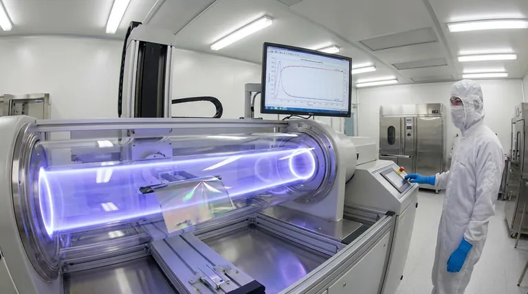
Visual Guide

Related Products
- RF PECVD System Radio Frequency Plasma Enhanced Chemical Vapor Deposition
- Inclined Rotary Plasma Enhanced Chemical Deposition PECVD Tube Furnace Machine
- Slide PECVD Tube Furnace with Liquid Gasifier PECVD Machine
- Inclined Rotary Plasma Enhanced Chemical Deposition PECVD Tube Furnace Machine
- Cylindrical Resonator MPCVD Machine System for Lab Diamond Growth
People Also Ask
- What are the advantages of PECVD in film deposition? Achieve Low-Temp, High-Quality Coatings
- What is the role of RF power in PECVD and how does the RF-PECVD process work? Master Thin Film Deposition Control
- What is PECVD specification? A Guide to Choosing the Right System for Your Lab
- How are deposition rates and film properties controlled in PECVD? Master Key Parameters for Optimal Thin Films
- How is silicon dioxide deposited from tetraethylorthosilicate (TEOS) in PECVD? Achieve Low-Temperature, High-Quality SiO2 Films


