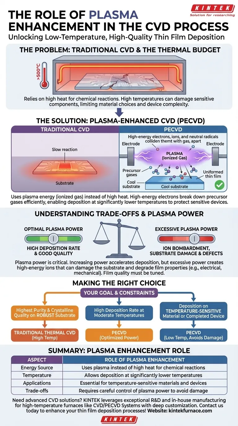
The primary role of plasma enhancement in the Chemical Vapor Deposition (CVD) process is to provide the energy needed for chemical reactions using an ionized gas—a plasma—instead of relying purely on high heat. This fundamental shift allows for the deposition of high-quality thin films at significantly lower temperatures, a critical capability for manufacturing modern electronic and optical devices.
Traditional CVD is limited by its "thermal budget"—the high temperatures required can damage or destroy sensitive components. Plasma enhancement bypasses this limitation, enabling the fabrication of complex, multi-layered devices that would otherwise be impossible.
The Problem with Traditional CVD: The Thermal Budget
To understand the value of plasma enhancement, we must first understand the limitations of conventional, thermally-driven CVD.
How Thermal CVD Works
In a standard CVD process, precursor gases are introduced into a vacuum chamber containing a substrate. The substrate is heated to very high temperatures, often several hundred degrees Celsius. This thermal energy breaks down the precursor gases, causing them to react and deposit a solid, thin film on the substrate's surface.
The Limitation of Heat
This reliance on high heat creates a significant constraint known as the thermal budget. If the substrate already contains fabricated circuits, transistors, or is made of a material with a low melting point (like a polymer), the high temperatures of thermal CVD can cause irreparable damage. This severely limits the types of materials and device structures that can be created.
How Plasma Enhancement Solves the Problem
Plasma-Enhanced Chemical Vapor Deposition (PECVD) provides a direct solution by replacing thermal energy with plasma energy.
Creating a Plasma
Instead of just heating the substrate, an electrical field (typically radio frequency, or RF) is applied to the precursor gases inside the chamber. This field energizes the gas, stripping electrons from the atoms and creating a highly reactive, ionized gas known as a plasma.
Energy Transfer Without Heat
This plasma is a soup of energetic electrons, ions, and neutral radicals. The high-energy electrons are the key players. They collide with the precursor gas molecules, breaking them apart into reactive species far more efficiently than heat alone.
These reactive species then travel to the much cooler substrate surface and form the desired thin film. The energy for the reaction comes from the plasma, not the heated substrate, allowing the deposition to occur at temperatures low enough to protect sensitive devices.
Understanding the Trade-offs of PECVD
While powerful, PECVD is not a universal solution. Its process parameters must be carefully controlled to achieve the desired outcome.
The Role of Plasma Power
Plasma power is a critical variable. Increasing the power energizes the plasma more intensely, which can accelerate the rate of deposition. This is often desirable for manufacturing throughput.
The Risk of High Power
However, excessive plasma power can be detrimental. It can create high-energy ions that bombard the substrate, causing physical damage or creating defects in the film's structure. This can degrade the film's electrical or mechanical properties and damage the underlying device.
Film Quality Considerations
PECVD films can also have different properties than their high-temperature counterparts. For example, they may incorporate more hydrogen or have a less dense atomic structure. These characteristics must be carefully managed through process tuning to ensure the film meets the required performance specifications.
Making the Right Choice for Your Goal
The decision to use thermal CVD or PECVD depends entirely on the application's constraints and the desired film properties.
- If your primary focus is the highest possible film purity and crystalline quality on a robust substrate: Traditional high-temperature CVD is often superior, provided the substrate can withstand the heat.
- If your primary focus is depositing a film onto a temperature-sensitive material or a completed device: PECVD is the necessary choice to avoid thermal damage.
- If your primary focus is achieving a high deposition rate at moderate temperatures: PECVD, with optimized plasma power, can provide an excellent balance of speed and quality.
Ultimately, plasma enhancement provides a critical degree of freedom, decoupling the chemical reaction energy from the substrate's temperature.
Summary Table:
| Aspect | Role of Plasma Enhancement |
|---|---|
| Energy Source | Uses plasma instead of high heat for chemical reactions |
| Temperature | Allows deposition at significantly lower temperatures |
| Applications | Essential for temperature-sensitive materials and devices |
| Trade-offs | Requires careful control of plasma power to avoid damage |
Need advanced CVD solutions for your lab? KINTEK leverages exceptional R&D and in-house manufacturing to provide high-temperature furnaces like CVD/PECVD Systems, with strong deep customization to meet your unique experimental needs. Contact us today to enhance your thin film deposition processes!
Visual Guide
Related Products
- RF PECVD System Radio Frequency Plasma Enhanced Chemical Vapor Deposition
- Slide PECVD Tube Furnace with Liquid Gasifier PECVD Machine
- Inclined Rotary Plasma Enhanced Chemical Deposition PECVD Tube Furnace Machine
- Inclined Rotary Plasma Enhanced Chemical Deposition PECVD Tube Furnace Machine
- MPCVD Machine System Reactor Bell-jar Resonator for Lab and Diamond Growth
People Also Ask
- How is silicon dioxide deposited from tetraethylorthosilicate (TEOS) in PECVD? Achieve Low-Temperature, High-Quality SiO2 Films
- How are deposition rates and film properties controlled in PECVD? Master Key Parameters for Optimal Thin Films
- What are some promising applications of PECVD-prepared 2D materials? Unlock Advanced Sensing and Optoelectronics
- What is RF in PECVD? A Critical Control for Plasma Deposition
- What are the key advantages of PECVD technology? Achieve Low-Temperature, High-Quality Thin Film Deposition