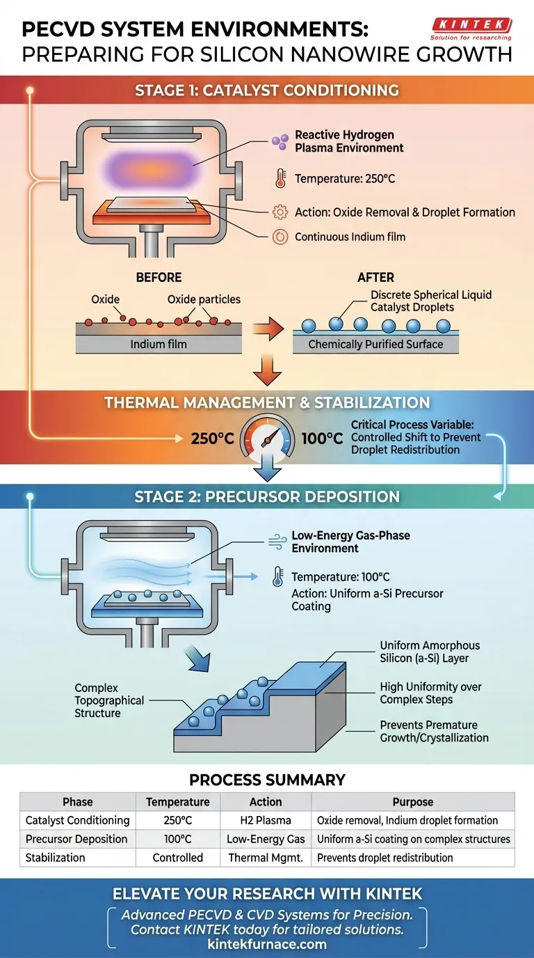
Prior to silicon nanowire growth, a Plasma Enhanced Chemical Vapor Deposition (PECVD) system establishes two distinct physical and chemical environments: a reactive hydrogen plasma environment at 250°C for catalyst conditioning, and a low-energy gas-phase environment at 100°C for uniform precursor deposition. These stages are critical for transforming metallic films into active catalysts and ensuring the silicon source material is correctly positioned for growth.
The PECVD system prepares the substrate by combining thermal energy with plasma interactions to physically shape catalyst droplets and chemically purify surfaces, while separately providing a low-temperature environment for precise material coating.

Conditioning the Catalyst Interface
The Hydrogen Plasma Environment
To prepare the substrate for growth, the PECVD system initiates a high-temperature phase at 250°C.
In this environment, the system introduces a hydrogen plasma treatment. This chemical environment is highly reactive, specifically targeting the surface of deposited Indium films.
Oxide Removal and Droplet Formation
The physical impact of this environment is transformative. The combination of thermal energy and plasma interaction forces the continuous Indium film to break apart.
This transforms the film into discrete spherical liquid catalyst droplets, which serve as the seeds for nanowire growth. Simultaneously, the hydrogen plasma chemically reacts with the surface to remove oxides, ensuring a pure interface between the catalyst and the substrate.
Establishing the Precursor Layer
Low-Energy Gas-Phase Environment
Once the catalyst is prepared, the PECVD system shifts to a significantly lower thermal profile of 100°C.
This environment is designed for the in-situ deposition of the growth material. Specifically, it facilitates the laying down of amorphous silicon (a-Si) precursor layers without triggering premature growth or crystallization.
Uniformity Across Complex Topography
The key physical characteristic of this 100°C environment is its high uniformity.
Because the gas-phase environment is low-energy, it allows the precursor material to settle evenly. This ensures that the a-Si layer effectively coats complex step-like topographical structures, preventing shadowing effects or uneven source material distribution.
Understanding the Process Trade-offs
Thermal Management Considerations
The transition between these two environments represents a critical process variable.
You must manage the shift from the 250°C catalyst treatment down to the 100°C precursor deposition carefully. Failing to stabilize the temperature at the lower setpoint could alter the viscosity or distribution of the liquid Indium droplets before the silicon layer is applied.
Surface Energy vs. Deposition Rate
The low-energy environment at 100°C prioritizes uniformity over deposition speed.
While this ensures excellent coverage on complex steps, it requires precise control of gas flow to maintain the amorphous nature of the silicon. Higher energies at this stage could inadvertently trigger crystallization in the a-Si layer, disrupting the intended nanowire growth mechanism later.
Making the Right Choice for Your Goal
To optimize your silicon nanowire growth, align your process parameters with your specific structural requirements:
- If your primary focus is Catalyst Activity: Prioritize the 250°C hydrogen plasma step to ensure complete oxide removal and the formation of perfectly spherical Indium droplets.
- If your primary focus is Complex Geometry Coverage: Rely on the 100°C low-energy environment to achieve a uniform a-Si coating over step-like structures without gaps.
Success in this process relies on the distinct separation and precise control of these two preparatory environments.
Summary Table:
| Environment Phase | Temperature | Chemical/Physical Action | Primary Purpose |
|---|---|---|---|
| Catalyst Conditioning | 250°C | Hydrogen Plasma Treatment | Oxide removal and formation of Indium catalyst droplets |
| Precursor Deposition | 100°C | Low-energy Gas-phase | Uniform amorphous silicon (a-Si) coating on complex structures |
| Stabilization | Controlled | Thermal Management | Prevents droplet redistribution and premature crystallization |
Elevate Your Nanotechnology Research with KINTEK
Precision is paramount in silicon nanowire growth. Whether you are conditioning catalysts or depositing uniform precursor layers, KINTEK’s advanced PECVD and CVD systems provide the thermal stability and plasma control necessary for your most complex topographical structures.
Backed by expert R&D and world-class manufacturing, we offer customizable high-temp lab furnaces—including Muffle, Tube, Rotary, and Vacuum systems—designed to meet the unique needs of cutting-edge material science.
Ready to optimize your deposition process? Contact KINTEK today to discuss how our tailored solutions can enhance your laboratory's efficiency and growth outcomes.
Visual Guide
References
- Lei Wu, Linwei Yu. Step-necking growth of silicon nanowire channels for high performance field effect transistors. DOI: 10.1038/s41467-025-56376-x
This article is also based on technical information from Kintek Furnace Knowledge Base .
Related Products
- RF PECVD System Radio Frequency Plasma Enhanced Chemical Vapor Deposition
- Slide PECVD Tube Furnace with Liquid Gasifier PECVD Machine
- Inclined Rotary Plasma Enhanced Chemical Deposition PECVD Tube Furnace Machine
- Inclined Rotary Plasma Enhanced Chemical Deposition PECVD Tube Furnace Machine
- 915MHz MPCVD Diamond Machine Microwave Plasma Chemical Vapor Deposition System Reactor
People Also Ask
- What is PECVD specification? A Guide to Choosing the Right System for Your Lab
- What are some promising applications of PECVD-prepared 2D materials? Unlock Advanced Sensing and Optoelectronics
- What are the advantages of PECVD in film deposition? Achieve Low-Temp, High-Quality Coatings
- What are the system specifications of the PECVD system? Unlock Precision Thin-Film Deposition
- How are deposition rates and film properties controlled in PECVD? Master Key Parameters for Optimal Thin Films


