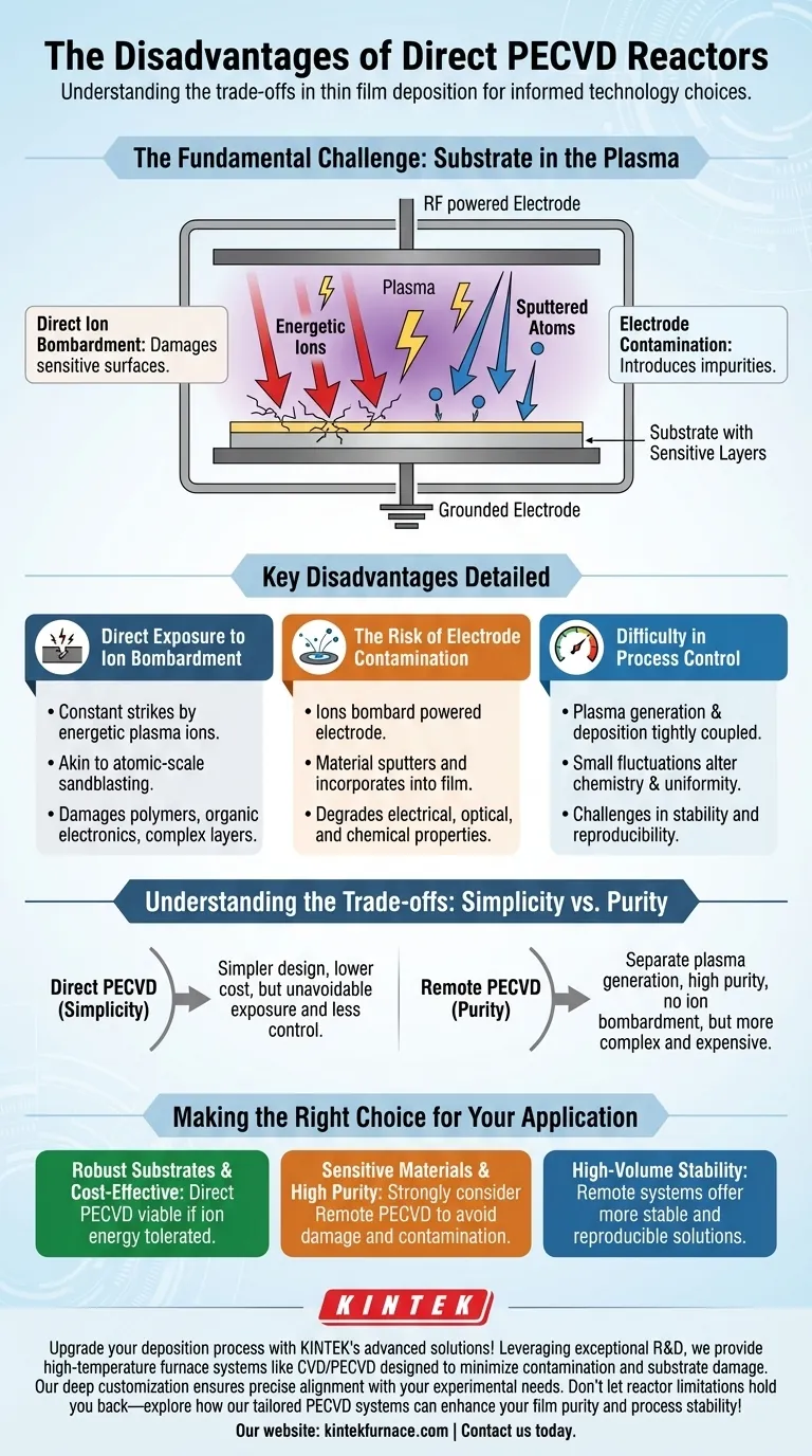
The primary disadvantages of a direct PECVD reactor are direct ion bombardment of the substrate and contamination from electrode erosion. Because the substrate is placed directly within the plasma field, it is exposed to energetic ions that can cause physical damage. Simultaneously, the electrodes themselves are bombarded, causing material to sputter off and become incorporated into the growing film as impurities.
The core issue with direct PECVD is its fundamental design: the substrate is immersed in the same plasma used to create the film precursors. This simplicity in setup creates an inherent trade-off, pitting deposition efficiency against the risk of substrate damage and reduced film purity.
The Fundamental Challenge: Substrate in the Plasma
The defining characteristic of a direct PECVD reactor, typically a capacitively coupled plasma (CCP) system, is that the substrate sits on one of the electrodes used to generate the plasma. This architecture is the direct cause of its main drawbacks.
Direct Exposure to Ion Bombardment
In a direct PECVD system, the substrate is constantly struck by energetic ions from the plasma. This is akin to a gentle, atomic-scale sandblasting.
While this ion energy can sometimes be beneficial for film density, it becomes a significant disadvantage when working with sensitive materials. This bombardment can damage the surface of polymers, organic electronics, or complex semiconductor device layers already present on the wafer.
The Risk of Electrode Contamination
The same ions that bombard the substrate also strike the powered electrode (and surrounding chamber walls). This bombardment can physically eject, or "sputter," atoms from the electrode material.
These sputtered atoms travel through the chamber and can be incorporated into the film as it grows on the substrate. This introduces metallic or other contaminants, which can severely degrade the film's desired electrical, optical, or chemical properties.
Difficulty in Process Control
Because the plasma generation and film deposition occur in the same physical space, the processes are tightly coupled. Small fluctuations in power, gas pressure, or temperature can alter the plasma's chemistry and uniformity.
This makes it challenging to achieve highly stable and reproducible conditions, especially when compared to systems where plasma generation is separated from the deposition chamber.
Understanding the Trade-offs: Simplicity vs. Purity
No technology is chosen without reason. The disadvantages of direct PECVD must be weighed against its benefits, which primarily revolve around simplicity and cost.
The Advantage of Simplicity
Direct PECVD reactors are often simpler in design and operation than their alternatives. With fewer components and a more straightforward setup, they can be less expensive to build and maintain. This makes them an attractive option for many applications where the highest purity or gentlest processing is not a strict requirement.
The Inherent Purity and Damage Problem
The trade-off for this simplicity is the unavoidable exposure of the substrate to the harsh plasma environment. You cannot decouple the plasma generation from the deposition process. This means you have less independent control over ion energy and flux at the substrate surface.
When to Consider Alternatives
The limitations of direct PECVD led to the development of indirect or remote PECVD systems. In these designs, the plasma is generated in a separate chamber, and only the desired reactive chemical species (radicals) are flowed over the substrate. This approach virtually eliminates both ion bombardment and electrode contamination, but at the cost of a more complex and expensive system.
Making the Right Choice for Your Application
Selecting the right deposition technology requires a clear understanding of your project's primary goal. The disadvantages of direct PECVD may be critical flaws for one application but acceptable trade-offs for another.
- If your primary focus is cost-effective deposition on robust substrates: Direct PECVD can be a viable and economical choice, especially if the material can withstand some ion energy.
- If your primary focus is depositing high-purity films on sensitive materials (like polymers or electronics): You should strongly consider an alternative like remote PECVD to avoid substrate damage and contamination from the electrodes.
- If your primary focus is achieving maximum process stability for high-volume manufacturing: The inherent coupling in direct PECVD requires exceptionally tight process control, and a remote system may offer a more stable and reproducible solution.
Ultimately, choosing the right tool depends on a clear-eyed assessment of the trade-offs between system cost, process complexity, and the final film quality your application demands.
Summary Table:
| Disadvantage | Impact |
|---|---|
| Direct Ion Bombardment | Physical damage to sensitive substrates like polymers and electronics |
| Electrode Contamination | Introduction of impurities, degrading film electrical and optical properties |
| Difficulty in Process Control | Challenges in achieving stable, reproducible conditions due to coupled processes |
Upgrade your deposition process with KINTEK's advanced solutions! Leveraging exceptional R&D and in-house manufacturing, we provide diverse laboratories with high-temperature furnace systems like CVD/PECVD Systems, designed to minimize contamination and substrate damage. Our strong deep customization capability ensures precise alignment with your unique experimental needs. Don't let reactor limitations hold you back—contact us today to explore how our tailored PECVD systems can enhance your film purity and process stability!
Visual Guide
Related Products
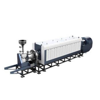
- Slide PECVD Tube Furnace with Liquid Gasifier PECVD Machine
- Inclined Rotary Plasma Enhanced Chemical Deposition PECVD Tube Furnace Machine
- Inclined Rotary Plasma Enhanced Chemical Deposition PECVD Tube Furnace Machine
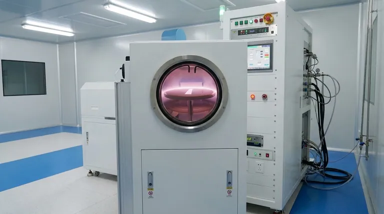
- RF PECVD System Radio Frequency Plasma Enhanced Chemical Vapor Deposition
- 915MHz MPCVD Diamond Machine Microwave Plasma Chemical Vapor Deposition System Reactor
People Also Ask
- What plasma source is used in PE-CVD tube furnaces? Unlock Low-Temperature, High-Quality Deposition
- How does a hydrogen reduction environment in an industrial tube furnace facilitate gold-copper alloy microspheres?
- What are the disadvantages of tube furnace cracking when processing heavy raw materials? Avoid Costly Downtime and Inefficiency
- What is plasma in the context of PECVD? Unlock Low-Temperature Thin Film Deposition
- How does PECVD equipment contribute to TOPCon bottom cells? Mastering Hydrogenation for Maximum Solar Efficiency