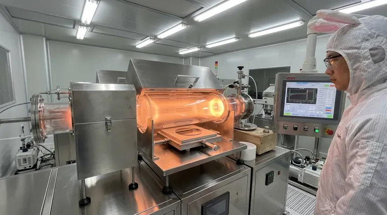
At its core, Plasma-Enhanced Chemical Vapor Deposition (PECVD) in a single wafer chamber is a process that uses an energized gas, or plasma, to break down chemical precursors. These reactive fragments then deposit onto a single, heated wafer to form a high-quality thin film. Unlike purely thermal methods, the plasma provides the energy for the chemical reaction, allowing the process to occur at significantly lower temperatures.
The fundamental advantage of PECVD is its use of plasma as an energy catalyst. This allows for the deposition of high-quality films at temperatures low enough to protect the delicate, pre-existing integrated circuits on the silicon wafer, a feat impossible with high-temperature thermal deposition methods.
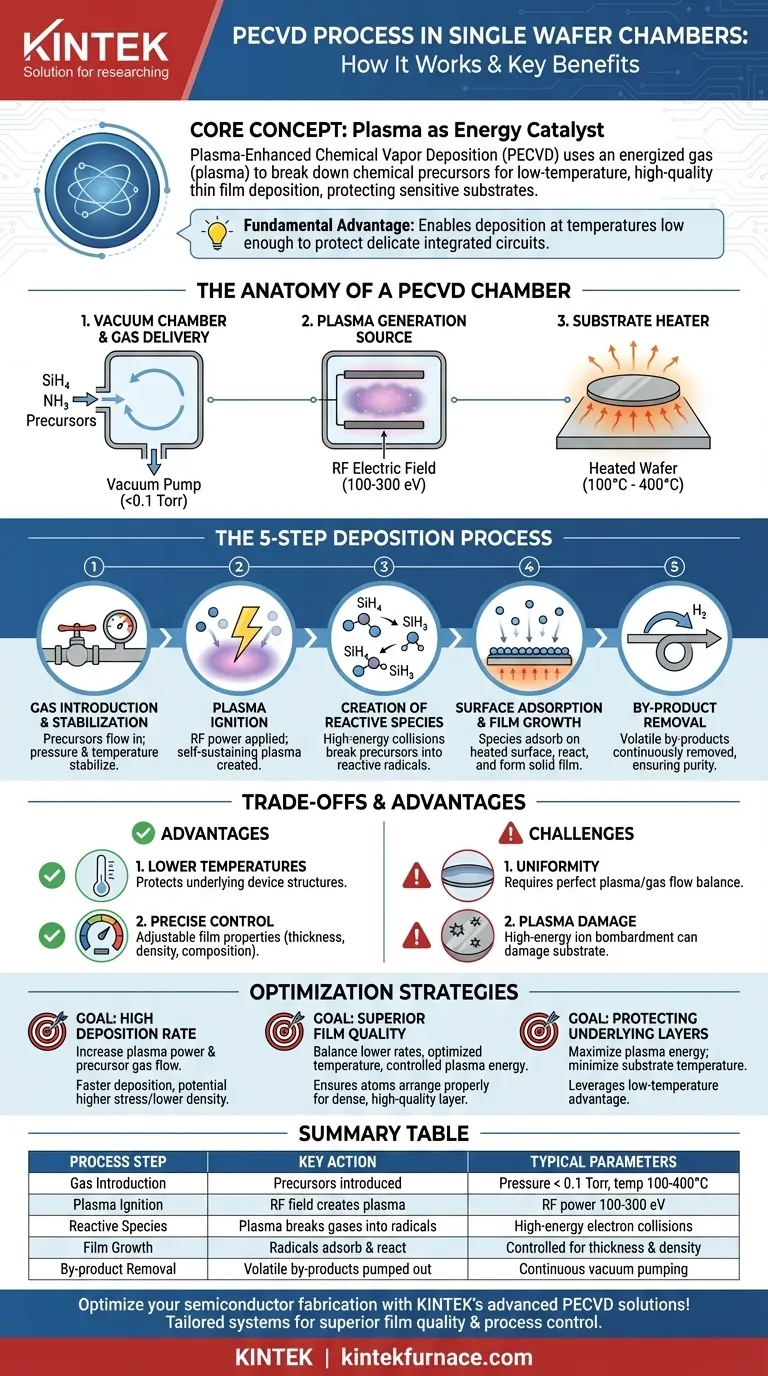
The Anatomy of a PECVD Chamber
To understand the process, we must first look at the critical components of the single-wafer system. Each part plays a precise role in creating a controlled environment for film growth.
The Vacuum Chamber and Gas Delivery
The entire process occurs within a sealed vacuum chamber. This controlled environment ensures process purity and allows for operation at very low pressures, typically below 0.1 Torr.
A sophisticated gas delivery system introduces precise amounts of precursor gases, such as silane (SiH₄) and ammonia (NH₃), into the chamber. These are the chemical building blocks of the final film.
The Plasma Generation Source
This is the heart of the PECVD system. It typically consists of two parallel electrodes, one of which holds the wafer. A high-frequency radio frequency (RF) electric field is applied between these electrodes.
This powerful electric field, often delivering energy in the range of 100-300 eV, energizes the gas, stripping electrons from atoms and creating the plasma. This is often referred to as a "capacitively coupled" or "glow" discharge.
The Substrate Heater
While PECVD is a "low-temperature" process, the wafer is still heated, typically to between 100°C and 400°C. This thermal energy is not enough to break down the precursor gases on its own, but it is crucial for controlling how the reactive fragments bond to the wafer surface and for influencing the final film quality.
The Step-by-Step Deposition Process
The deposition of a film via PECVD follows a precise and rapid sequence of events within the chamber.
Step 1: Gas Introduction and Stabilization
Precursor gases are flowed into the vacuum chamber at a controlled rate. The system pressure and wafer temperature are brought to their target setpoints and stabilized.
Step 2: Plasma Ignition
The RF electric field is applied to the electrodes. This field accelerates free electrons in the gas, causing them to collide with neutral gas molecules. These energetic collisions create a self-sustaining plasma—a glowing, highly reactive mix of ions, electrons, and neutral radicals.
Step 3: Creation of Reactive Species
Within the plasma, the stable precursor gases are broken apart by high-energy electron collisions. A stable gas like silane (SiH₄) is fragmented into highly reactive species (radicals) like SiH₃ and SiH₂. These fragments are chemically unstable and eager to react.
Step 4: Surface Adsorption and Film Growth
These reactive species diffuse through the chamber and land on the heated wafer surface, a process called adsorption.
Once on the surface, they move around and react with each other, bonding to form a stable, solid thin film. The substrate heating provides the necessary surface mobility for the atoms to arrange into a dense, high-quality layer.
Step 5: By-product Removal
The chemical reactions on the surface also create volatile by-products (for example, H₂ gas). These by-products do not stick to the wafer and are continuously removed from the chamber by the vacuum pump, ensuring a pure film.
Understanding the Trade-offs and Advantages
PECVD is a powerful technique, but its application involves balancing competing factors. Understanding these trade-offs is key to process mastery.
Key Advantage: Lower Temperature
The primary reason to use PECVD is its ability to deposit films at low temperatures. The plasma provides the activation energy that would otherwise have to come from extreme heat, thus protecting sensitive device structures already built on the wafer.
Key Advantage: Control Over Film Properties
By adjusting plasma power, gas flow rates, pressure, and temperature, an engineer can precisely control the film's properties. This includes its thickness, density, chemical composition, and internal stress, which is critical for device performance.
Challenge: Uniformity
A major engineering challenge in single-wafer PECVD is ensuring the plasma density and gas flow are perfectly uniform from the center of the wafer to its edge. Any non-uniformity will result in a film of varying thickness or quality across the wafer.
Pitfall: Plasma-Induced Damage
While the plasma is essential, its high-energy ions can physically bombard the wafer surface. If not properly controlled, this bombardment can cause damage to the substrate or the film itself, compromising device reliability.
Making the Right Choice for Your Goal
Optimizing a PECVD process requires aligning the process parameters with the desired outcome for the film.
- If your primary focus is a high deposition rate: Increasing plasma power and precursor gas flows will generally deposit the film faster, but this may come at the cost of higher film stress or lower density.
- If your primary focus is superior film quality: This demands a careful balance of lower deposition rates, optimized temperature, and controlled plasma energy to ensure atoms have time to arrange properly on the surface.
- If your primary focus is protecting underlying layers: The goal is to maximize the energy delivered by the plasma while keeping the substrate temperature as low as possible, leveraging the core strength of PECVD.
Understanding these fundamental principles transforms the PECVD process from a black box into a precise and adaptable manufacturing tool.
Summary Table:
| Process Step | Key Action | Typical Parameters |
|---|---|---|
| Gas Introduction | Precursor gases (e.g., SiH₄, NH₃) are introduced | Pressure < 0.1 Torr, temperature 100-400°C |
| Plasma Ignition | RF electric field creates plasma | RF power 100-300 eV |
| Reactive Species | Plasma breaks gases into radicals (e.g., SiH₃) | High-energy electron collisions |
| Film Growth | Radicals adsorb and react on heated wafer | Controlled for thickness and density |
| By-product Removal | Volatile by-products (e.g., H₂) are pumped out | Continuous vacuum pumping |
Optimize your semiconductor fabrication with KINTEK's advanced PECVD solutions! Leveraging exceptional R&D and in-house manufacturing, we provide diverse laboratories with tailored high-temperature furnace systems, including our CVD/PECVD Systems. Our strong deep customization capability ensures precise alignment with your unique experimental needs, delivering superior film quality, uniformity, and process control. Contact us today to discuss how our expertise can enhance your thin film deposition processes and protect your sensitive device layers!
Visual Guide
Related Products
- Slide PECVD Tube Furnace with Liquid Gasifier PECVD Machine
- RF PECVD System Radio Frequency Plasma Enhanced Chemical Vapor Deposition
- Inclined Rotary Plasma Enhanced Chemical Deposition PECVD Tube Furnace Machine
- Inclined Rotary Plasma Enhanced Chemical Deposition PECVD Tube Furnace Machine
- Split Chamber CVD Tube Furnace with Vacuum Station CVD Machine
People Also Ask
- What is plasma in the context of PECVD? Unlock Low-Temperature Thin Film Deposition
- How does a hydrogen reduction environment in an industrial tube furnace facilitate gold-copper alloy microspheres?
- How does PECVD equipment contribute to TOPCon bottom cells? Mastering Hydrogenation for Maximum Solar Efficiency
- What role does a Tube Furnace play in the CVD growth of carbon nanotubes? Achieve High-Purity CNT Synthesis
- What plasma source is used in PE-CVD tube furnaces? Unlock Low-Temperature, High-Quality Deposition


