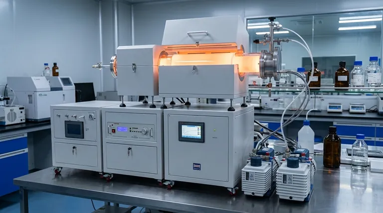
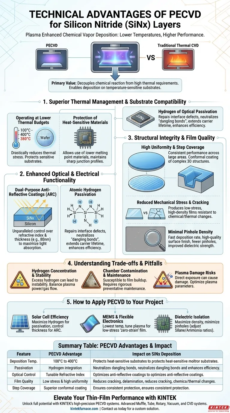
Plasma Enhanced Chemical Vapor Deposition (PECVD) systems provide a critical technical advantage by utilizing plasma energy to drive chemical reactions at significantly lower temperatures than conventional thermal CVD. When depositing silicon nitride (SiNx), this process enables precise control over film thickness and refractive index while facilitating hydrogen passivation, which is essential for improving the electrical performance and efficiency of semiconductor devices and solar cells.
PECVD's primary value lies in its ability to decouple the chemical reaction from high thermal requirements, allowing for the deposition of high-quality, low-stress SiNx films on temperature-sensitive substrates. This technique simultaneously serves as a functional anti-reflective coating and a critical passivation layer.
Superior Thermal Management and Substrate Compatibility
Operating at Lower Thermal Budgets
Standard Chemical Vapor Deposition often requires high temperatures that can damage sensitive substrates or pre-existing device layers. PECVD operates effectively between 100°C and 400°C (commonly around 380°C), drastically reducing the thermal stress applied to the wafer.
Protection of Heat-Sensitive Materials
By maintaining a lower basic temperature requirement, PECVD allows for the use of materials with lower melting points or those prone to diffusion at high heat. This flexibility is vital for advanced electronics where maintaining sharp junction profiles is a priority.
Enhanced Optical and Electrical Functionality
Dual-Purpose Anti-Reflective Coatings (ARC)
PECVD SiNx layers are frequently used as anti-reflective coatings due to the system's unparalleled control over the film's refractive index and thickness. This precision allows engineers to target specific wavelengths, such as 80nm layers, to maximize light absorption through coherent interference.
Atomic Hydrogen Passivation
During the PECVD process, hydrogen atoms are naturally introduced into the SiNx film and the underlying silicon interface. This hydrogen passivation repairs interface defects and neutralizes "dangling bonds," which significantly extends carrier lifetime and enhances photoelectric conversion efficiency.
Structural Integrity and Film Quality
High Uniformity and Step Coverage
PECVD systems produce films with high uniformity across large-area substrates, ensuring consistent performance in mass production. The process also provides superior step coverage, meaning the SiNx layer can conformally coat complex 3D structures without leaving gaps or thin spots.
Reduced Mechanical Stress and Cracking
Unlike traditional CVD, PECVD produces low-stress films that are less susceptible to cracking or delamination. The resulting SiNx layers exhibit high cross-linking and density, providing robust resistance to subsequent chemical or thermal changes.
Minimal Pinhole Density
The plasma-enhanced environment facilitates a fast deposition rate while maintaining a high-quality surface finish. This leads to films with fewer pinholes, which improves the dielectric strength and protective qualities of the SiNx layer.
Understanding the Trade-offs and Pitfalls
Hydrogen Concentration and Stability
While hydrogen is beneficial for passivation, an excess of hydrogen in the SiNx film can lead to long-term stability issues or "bubbling" during subsequent high-temperature steps. Engineers must carefully balance the plasma power and gas flow to achieve the desired hydrogen content.
Chamber Contamination and Maintenance
PECVD chambers are susceptible to thick film buildup on the walls, which can flake off and contaminate the substrate. Although these systems are relatively easy to clean compared to some alternatives, a rigorous preventative maintenance schedule is required to ensure high yields.
Plasma Damage Risks
Direct exposure to high-energy plasma can occasionally cause "plasma damage" to sensitive gate oxides or surface structures. Optimizing the plasma frequency and power is necessary to minimize ion bombardment while maintaining deposition rates.
How to Apply PECVD to Your Project
When integrating PECVD SiNx into your manufacturing flow, your specific technical goals will dictate the system parameters.
- If your primary focus is solar cell efficiency: Optimize the deposition parameters to maximize hydrogen content for surface passivation while strictly controlling thickness to 80nm for anti-reflection.
- If your primary focus is MEMS or flexible electronics: Prioritize the lowest possible deposition temperature and focus on tuning the plasma power to achieve a low-stress, "zero-strain" film to prevent substrate warping.
- If your primary focus is dielectric isolation: Focus on maximizing film density and minimizing pinhole count by adjusting the precursor gas ratios (typically Silane and Ammonia) to ensure high breakdown voltage.
By leveraging the low-temperature versatility of PECVD, you can achieve a high-performance SiNx layer that protects, passivates, and optimizes your device's architecture.
Summary Table:
| Feature | PECVD Advantage | Impact on SiNx Deposition |
|---|---|---|
| Deposition Temp. | 100°C to 400°C | Protects heat-sensitive substrates and prevents diffusion. |
| Passivation | Hydrogen integration | Neutralizes dangling bonds and improves electrical efficiency. |
| Optical Control | Tunable Refractive Index | Optimizes anti-reflective coatings (ARC) for solar cells. |
| Film Quality | Low stress & high uniformity | Reduces cracking, delamination, and pinhole density. |
| Step Coverage | Superior conformal coating | Ensures consistent protection across complex 3D structures. |
Elevate Your Thin-Film Performance with KINTEK
Unlock the full potential of your semiconductor or solar cell production with KINTEK’s high-precision PECVD systems. Backed by expert R&D and manufacturing, we provide advanced Muffle, Tube, Rotary, Vacuum, and CVD systems tailored for your unique lab and industrial needs.
Our customizable high-temperature solutions ensure:
- Precision Control: Achieve exact film thickness and refractive index for SiNx layers.
- Unmatched Versatility: Ideal for MEMS, flexible electronics, and dielectric isolation.
- Expert Support: Benefit from our deep engineering expertise in plasma-enhanced technology.
Ready to optimize your deposition process for superior quality and lower thermal budgets? Contact us today to discuss your custom solution.
Visual Guide
References
- Hakim Korichi, Ahmed Baha-Eddine Bensdira. Investigating the influence of boron diffusion temperature on the performance of n-type PERT monofacial solar cells with reduced thermal steps. DOI: 10.35784/iapgos.6599
This article is also based on technical information from Kintek Furnace Knowledge Base .
Related Products
- RF PECVD System Radio Frequency Plasma Enhanced Chemical Vapor Deposition
- Slide PECVD Tube Furnace with Liquid Gasifier PECVD Machine
- Inclined Rotary Plasma Enhanced Chemical Deposition PECVD Tube Furnace Machine
- Inclined Rotary Plasma Enhanced Chemical Deposition PECVD Tube Furnace Machine
- 915MHz MPCVD Diamond Machine Microwave Plasma Chemical Vapor Deposition System Reactor
People Also Ask
- What are the key advantages of PECVD technology? Achieve Low-Temperature, High-Quality Thin Film Deposition
- What is PECVD specification? A Guide to Choosing the Right System for Your Lab
- What are the advantages of PECVD in film deposition? Achieve Low-Temp, High-Quality Coatings
- What is RF in PECVD? A Critical Control for Plasma Deposition
- What are some promising applications of PECVD-prepared 2D materials? Unlock Advanced Sensing and Optoelectronics


