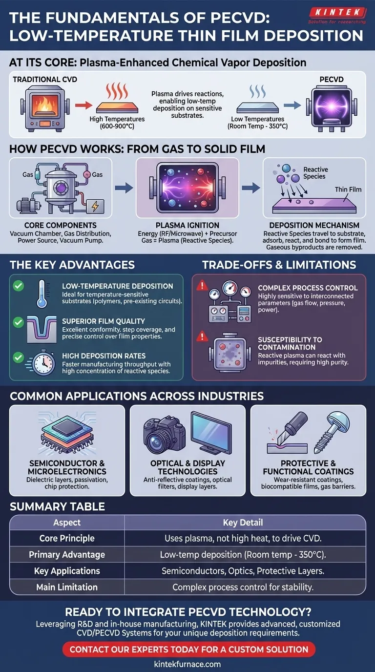
At its core, Plasma-Enhanced Chemical Vapor Deposition (PECVD) is a process used to deposit high-quality thin films onto a substrate. Unlike traditional Chemical Vapor Deposition (CVD) which relies on high temperatures, PECVD uses an energized gas, or plasma, to drive the chemical reactions. This allows for deposition to occur at significantly lower temperatures, making it a critical technology for manufacturing modern electronics and advanced materials.
The fundamental advantage of PECVD is its ability to decouple the energy required for deposition from thermal heat. By using a plasma to activate precursor gases, it enables the creation of dense, high-performance films on materials that would be damaged or destroyed by high-temperature processes.
How PECVD Works: From Gas to Solid Film
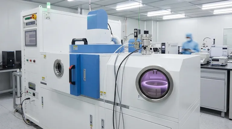
PECVD is a vacuum deposition technique that involves a sequence of controlled physical and chemical events. The process is contained entirely within a sealed chamber to ensure purity and control.
The Core Components
A PECVD system is built around a vacuum chamber which holds the substrate. This chamber is supported by a vacuum pump system to remove air and control pressure, a gas distribution system to introduce precise precursor gases, and a power source (typically radio frequency or microwave) to generate the plasma.
The Plasma Ignition
The process begins by introducing specific precursor gases into the low-pressure chamber. The power source is then activated, applying energy to the gas and igniting it into a plasma. A plasma is an ionized state of matter containing a mix of ions, electrons, and highly reactive neutral species called radicals.
The Deposition Mechanism
This plasma is the engine of the PECVD process. The high-energy species within the plasma bombard and break down the stable precursor gas molecules into reactive species. These highly reactive fragments then travel to the surface of the substrate, where they adsorb, react, and bond to form the desired solid film. Gaseous byproducts from these surface reactions are desorbed and removed by the vacuum system.
Why Choose PECVD? The Key Advantages
The use of plasma instead of high heat provides several distinct and powerful advantages over conventional thermal CVD and other deposition methods.
The Low-Temperature Advantage
This is the primary reason for PECVD's widespread use. Deposition can occur at temperatures from room temperature up to around 350°C, whereas traditional CVD often requires temperatures of 600-900°C or higher. This makes PECVD essential for depositing films on temperature-sensitive substrates like polymers, plastics, or semiconductor wafers with pre-existing integrated circuits.
Superior Film Quality and Control
PECVD offers excellent conformity, meaning it can evenly coat complex, non-flat surfaces and deep trenches. This "step coverage" is far superior to line-of-sight techniques like Physical Vapor Deposition (PVD). The process also allows for precise control over film properties like density, stress, and chemical composition.
High Deposition Rates
By creating a high concentration of reactive species in the plasma, PECVD can often achieve higher deposition rates than other low-temperature techniques, improving manufacturing throughput.
Understanding the Trade-offs and Limitations
While powerful, PECVD is not a universal solution. It comes with its own set of technical challenges that demand expert control.
The Challenge of Process Control
The biggest limitation of PECVD is its complexity. Film quality is highly sensitive to a range of interconnected parameters, including gas flow rates, pressure, chamber temperature, and plasma power. Achieving stable and reproducible deposition requires sophisticated control systems and deep process expertise.
Susceptibility to Contamination
The highly reactive nature of the plasma means it can react with any impurities present in the chamber, such as residual water vapor or nitrogen. This makes the process highly susceptible to contamination, which can degrade film quality. High-purity precursor gases and a robust vacuum system are non-negotiable.
Common Applications Across Industries
The unique capabilities of PECVD have made it a cornerstone technology in several high-tech fields.
In Semiconductor and Microelectronics
PECVD is essential for fabricating microchips. It is used to deposit dielectric (insulating) layers like silicon dioxide and silicon nitride, as well as passivation layers that protect the chip from the environment.
For Optical and Display Technologies
The precise control over film properties makes PECVD ideal for creating multi-layer optical coatings, such as anti-reflective coatings on lenses and filters. It is also used extensively in manufacturing flat panel displays.
For Protective and Functional Coatings
The process is used to create hard, wear-resistant coatings on cutting tools, biocompatible coatings on medical implants, and impermeable gas barrier films used in flexible electronics and advanced food packaging.
Making the Right Choice for Your Goal
Selecting a deposition method depends entirely on the material properties, substrate limitations, and performance requirements of your specific application.
- If your primary focus is depositing on temperature-sensitive substrates: PECVD is the definitive choice, as its plasma-driven chemistry avoids the need for damaging high heat.
- If your primary focus is achieving complex, conformal coatings: PECVD provides superior coverage over intricate 3D geometries compared to line-of-sight methods.
- If your primary focus is process simplicity or lowest initial cost: Be aware that PECVD requires significant investment in precision equipment and process control, and may be more complex than alternatives like PVD.
Ultimately, PECVD is an enabling technology that allows engineers and scientists to build advanced devices and materials that would otherwise be impossible.
Summary Table:
| Aspect | Key Detail |
|---|---|
| Core Principle | Uses plasma, not high heat, to drive chemical vapor deposition. |
| Primary Advantage | Enables deposition at low temperatures (room temp to ~350°C). |
| Key Applications | Semiconductor fabrication, optical coatings, protective layers. |
| Main Limitation | Complex process control required for stable, reproducible results. |
Ready to integrate PECVD technology into your R&D or production line?
Leveraging exceptional R&D and in-house manufacturing, KINTEK provides diverse laboratories with advanced high-temperature furnace solutions, including specialized CVD/PECVD Systems. Our strong deep customization capability allows us to precisely tailor equipment to meet your unique experimental and production requirements for thin film deposition.
Contact our experts today to discuss how a customized PECVD solution can accelerate your project.
Visual Guide
Related Products
- Slide PECVD Tube Furnace with Liquid Gasifier PECVD Machine
- RF PECVD System Radio Frequency Plasma Enhanced Chemical Vapor Deposition
- Inclined Rotary Plasma Enhanced Chemical Deposition PECVD Tube Furnace Machine
- Inclined Rotary Plasma Enhanced Chemical Deposition PECVD Tube Furnace Machine
- Multi Heating Zones CVD Tube Furnace Machine for Chemical Vapor Deposition Equipment
People Also Ask
- What are the disadvantages of tube furnace cracking when processing heavy raw materials? Avoid Costly Downtime and Inefficiency
- What is plasma in the context of PECVD? Unlock Low-Temperature Thin Film Deposition
- What are the typical conditions for plasma-enhanced CVD processes? Achieve Low-Temperature Thin Film Deposition
- What are the advantages of using a tube furnace CVD system for Cu(111)/graphene? Superior Scalability and Quality
- How does a hydrogen reduction environment in an industrial tube furnace facilitate gold-copper alloy microspheres?


