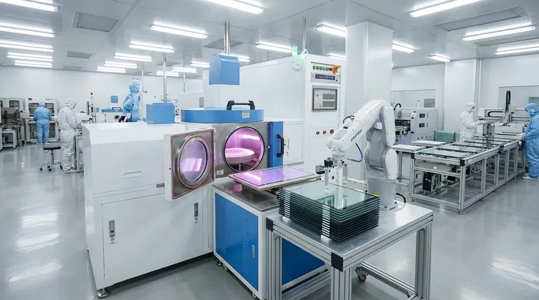
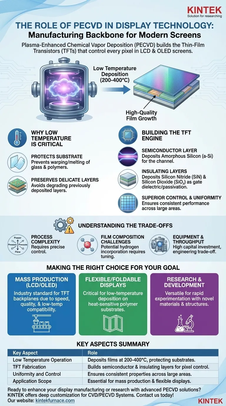
In essence, Plasma-Enhanced Chemical Vapor Deposition (PECVD) is the manufacturing backbone for modern high-resolution displays. It is the critical process used to deposit the ultra-thin layers of semiconductor and insulating materials that form the microscopic switches—known as Thin-Film Transistors (TFTs)—controlling every single pixel in an LCD or OLED screen.
The core challenge in display manufacturing is building complex, high-performance electronics on large, heat-sensitive glass or plastic substrates. PECVD solves this by using an energy-rich plasma to deposit high-quality films at low temperatures, a task impossible for traditional high-heat methods.
Why Low Temperature is the Deciding Factor
The primary reason PECVD is indispensable for display manufacturing is its ability to operate at low temperatures. Traditional Chemical Vapor Deposition (CVD) requires very high heat to trigger the chemical reactions needed to form a film.
Protecting the Display Substrate
Display panels are made from large sheets of glass or, for flexible displays, polymer plastics. These materials cannot withstand the high temperatures (often >800°C) of older fabrication methods without warping, melting, or breaking.
PECVD operates at much lower temperatures (typically 200-400°C), well within the tolerance of these substrates.
Preserving Delicate Layers
Displays are built layer by layer. Once one sensitive electronic layer is deposited, subjecting the panel to high temperatures to add the next layer would destroy the work already done.
The low thermal budget of PECVD ensures that each new layer can be added without degrading the fragile, complex circuitry underneath it.
Building the Engine of the Pixel: The Thin-Film Transistor
Every pixel on a modern screen needs its own dedicated switch to turn it on, off, or set its brightness. This switch is a Thin-Film Transistor (TFT), and PECVD is used to build its most crucial components. Think of a TFT as the microscopic gatekeeper for the light of each pixel.
Depositing the Semiconductor Layer
The heart of the TFT is its semiconductor channel, most commonly made of amorphous silicon (a-Si). PECVD is the industry-standard method for depositing this a-Si layer with high uniformity over a very large area.
Creating Critical Insulating Layers
A transistor requires insulating layers to function correctly. PECVD is used to deposit materials like silicon nitride (SiN) and silicon dioxide (SiO₂).
These films serve as the gate dielectric, which controls the flow of current in the transistor, and as passivation layers, which protect the transistor from environmental contamination.
Superior Control and Uniformity
The plasma process gives manufacturers exceptional control over the film's properties, such as its density, stress, and electrical characteristics. This ensures that the millions of TFTs across a display perform uniformly, preventing defects and ensuring a consistent, high-quality image.
Understanding the Trade-offs
While dominant, PECVD is a sophisticated process with inherent complexities. Recognizing its limitations is key to understanding its application.
Process Complexity
The use of plasma adds many variables to the deposition process, including power, pressure, gas flow, and frequency. Maintaining precise control over these variables is critical to achieving repeatable, high-quality results and avoiding film defects.
Film Composition Challenges
Because PECVD uses reactive gases broken down by plasma, elements from those gases (like hydrogen) can become incorporated into the deposited film. While this is often managed, excess hydrogen can impact the electronic performance of the semiconductor layer, requiring careful process tuning.
Equipment and Throughput
PECVD systems are complex vacuum chambers that represent a significant capital investment. While they offer high deposition rates compared to some alternatives, balancing deposition speed with film quality is a constant engineering trade-off in mass production.
Making the Right Choice for Your Goal
PECVD's role is defined by the specific goal of the manufacturing process, from mass production to next-generation research.
- If your primary focus is mass-producing standard LCD or OLED displays: PECVD is the non-negotiable industry standard for creating the TFT backplane due to its unmatched balance of speed, quality, and low-temperature compatibility.
- If your primary focus is developing flexible or foldable displays: PECVD's low-temperature capability is even more critical, as it is one of the few technologies that can deposit high-quality electronic films onto heat-sensitive polymer substrates.
- If your primary focus is research and development: The versatility of PECVD allows for rapid experimentation with a wide range of novel materials and device structures, from advanced semiconductors to specialized optical or protective coatings.
Ultimately, understanding PECVD is understanding the foundational process that enables the vibrant, high-resolution screens that are integral to our daily lives.
Summary Table:
| Key Aspect | Role in Display Technology |
|---|---|
| Low Temperature Operation | Deposits films at 200-400°C, preventing damage to heat-sensitive glass or plastic substrates. |
| TFT Fabrication | Builds semiconductor (e.g., amorphous silicon) and insulating layers (e.g., silicon nitride) for pixel control. |
| Uniformity and Control | Ensures consistent film properties across large areas, reducing defects and improving image quality. |
| Application Scope | Essential for mass production of LCD/OLED displays and development of flexible displays. |
Ready to enhance your display manufacturing or research with advanced PECVD solutions? KINTEK leverages exceptional R&D and in-house manufacturing to provide high-temperature furnace solutions, including CVD/PECVD Systems, tailored for diverse laboratories. Our strong deep customization capability ensures we meet your unique experimental needs—contact us today to discuss how we can optimize your processes for superior results!
Visual Guide
Related Products
- RF PECVD System Radio Frequency Plasma Enhanced Chemical Vapor Deposition
- Slide PECVD Tube Furnace with Liquid Gasifier PECVD Machine
- Inclined Rotary Plasma Enhanced Chemical Deposition PECVD Tube Furnace Machine
- Inclined Rotary Plasma Enhanced Chemical Deposition PECVD Tube Furnace Machine
- Cylindrical Resonator MPCVD Machine System for Lab Diamond Growth
People Also Ask
- What is RF in PECVD? A Critical Control for Plasma Deposition
- What are some promising applications of PECVD-prepared 2D materials? Unlock Advanced Sensing and Optoelectronics
- What is PECVD specification? A Guide to Choosing the Right System for Your Lab
- What are the applications of plasma enhanced chemical vapor deposition? Key Uses in Electronics, Optics & Materials
- What are the advantages of PECVD in film deposition? Achieve Low-Temp, High-Quality Coatings


