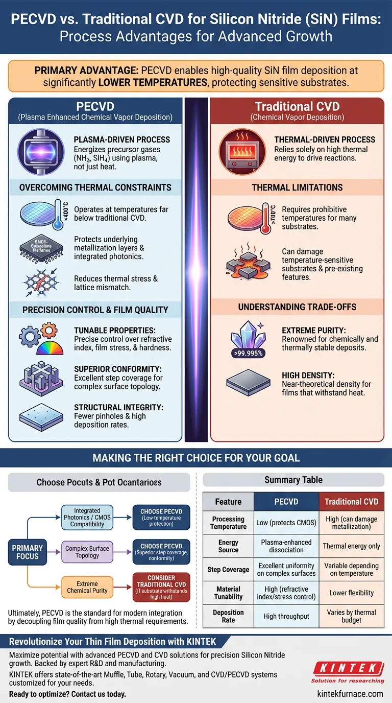
The primary advantage of Plasma Enhanced Chemical Vapor Deposition (PECVD) over traditional CVD is the ability to deposit high-quality Silicon Nitride (SiN) films at significantly lower temperatures.
By introducing plasma into the reaction chamber, PECVD energizes precursor gases—specifically ammonia (NH3) and silane (SiH4)—to initiate chemical reactions that would otherwise require high thermal energy. This capability is critical for applications where preserving the integrity of the substrate is paramount.
Core Takeaway Traditional CVD relies on heat to drive reactions, often limiting its use with temperature-sensitive substrates. PECVD circumvents this by using plasma to drive deposition, enabling the integration of high-quality Silicon Nitride films onto CMOS-compatible platforms without damaging underlying metallization layers or delicate device structures.
Overcoming Thermal Constraints
The Plasma Mechanism
In a standard CVD process, thermal energy is the sole driver for breaking down chemical precursors. This often necessitates temperatures that are prohibitive for many advanced applications.
PECVD alters this dynamic by using plasma to dissociate gases like silane and ammonia. This allows the deposition of Silicon Nitride to occur at temperatures far below those required by thermal CVD.
Protecting Sensitive Architectures
The lower operating temperature is the defining enabler for integrated photonics. High temperatures can degrade pre-existing features on a wafer.
PECVD allows for the growth of SiN films on CMOS-compatible platforms without compromising the underlying metallization layers. It ensures that the heat budget of the deposition process does not destroy the precise electronic structures already fabricated on the chip.
Reducing Thermal Stress
Beyond preventing immediate damage, lower processing temperatures reduce long-term structural risks.
High-temperature processing often leads to thermal stress and lattice mismatch between the film and the substrate. By operating at cooler temperatures, PECVD mitigates these adverse effects, resulting in better adhesion and mechanical stability.
Precision Control and Film Quality
Tunable Material Properties
PECVD offers superior control over the physical characteristics of the deposited film.
Engineers can tightly regulate critical properties such as refractive index, film stress, and hardness. This level of tunability is essential for optimizing optical performance in photonic devices.
Superior Conformity
Depositing films on uneven or complex surfaces is a common challenge in microfabrication.
PECVD provides excellent step coverage and conformity. This ensures that the Silicon Nitride film coats the contours of the substrate uniformly, which is vital for the reliability of 3D structures.
Structural Integrity and Speed
The process yields films with high density and significantly fewer pinholes compared to standard techniques.
Furthermore, PECVD typically achieves high deposition rates. This combination of speed and low-defect density improves both the throughput of the manufacturing process and the final reliability of the device.
Understanding the Trade-offs
While PECVD is superior for temperature-sensitive applications, it is important to recognize the strengths of traditional CVD to ensure an objective selection process.
Traditional thermal CVD is renowned for producing deposits of extreme purity (often exceeding 99.995%). It creates coatings that are chemically and thermally stable, often with near-theoretical density.
If a substrate can withstand high heat, traditional CVD may offer marginal gains in absolute purity. However, for modern integrated circuits and photonics, the thermal penalty of traditional CVD is usually too high to pay.
Making the Right Choice for Your Goal
To select the correct deposition method, you must weigh your thermal budget against your purity requirements.
- If your primary focus is Integrated Photonics or CMOS Compatibility: Choose PECVD to ensure low-temperature processing that protects underlying metallization layers and sensitive device structures.
- If your primary focus is Complex Surface Topology: Choose PECVD for its superior step coverage, low pinhole density, and ability to uniformly coat uneven surfaces.
- If your primary focus is Extreme Chemical Purity: Consider traditional CVD only if the substrate can withstand significantly higher processing temperatures without degradation.
Ultimately, PECVD is the standard for modern integration because it decouples film quality from high thermal requirements, allowing advanced material growth on delicate platforms.
Summary Table:
| Feature | PECVD | Traditional CVD |
|---|---|---|
| Processing Temperature | Low (protects CMOS layers) | High (can damage metallization) |
| Energy Source | Plasma-enhanced dissociation | Thermal energy only |
| Step Coverage | Excellent uniformity on complex surfaces | Variable depending on temperature |
| Material Tunability | High (refractive index/stress control) | Lower flexibility |
| Deposition Rate | High throughput | Varies by thermal budget |
Revolutionize Your Thin Film Deposition with KINTEK
Maximize your lab's potential with advanced PECVD and CVD solutions tailored for precision Silicon Nitride growth. Backed by expert R&D and manufacturing, KINTEK offers state-of-the-art Muffle, Tube, Rotary, Vacuum, and CVD/PECVD systems—all customizable to meet your unique research and industrial needs. Whether you are developing CMOS-compatible platforms or integrated photonics, our high-temp lab furnaces ensure superior film integrity and process stability.
Ready to optimize your fabrication workflow? Contact us today to speak with an expert and find the perfect system for your application!
Visual Guide
References
- Zachariah O. Martin, Vladimir M. Shalaev. Single-photon emitters in PECVD-grown silicon nitride films: from material growth to photophysical properties. DOI: 10.1515/nanoph-2024-0506
This article is also based on technical information from Kintek Furnace Knowledge Base .
Related Products
- RF PECVD System Radio Frequency Plasma Enhanced Chemical Vapor Deposition
- Slide PECVD Tube Furnace with Liquid Gasifier PECVD Machine
- Inclined Rotary Plasma Enhanced Chemical Deposition PECVD Tube Furnace Machine
- Inclined Rotary Plasma Enhanced Chemical Deposition PECVD Tube Furnace Machine
- 915MHz MPCVD Diamond Machine Microwave Plasma Chemical Vapor Deposition System Reactor
People Also Ask
- What are the system specifications of the PECVD system? Unlock Precision Thin-Film Deposition
- What is PECVD specification? A Guide to Choosing the Right System for Your Lab
- What are the limitations of PECVD? Overcome Process Control and Cost Challenges
- What are the key advantages of PECVD technology? Achieve Low-Temperature, High-Quality Thin Film Deposition
- What is the role of RF power in PECVD and how does the RF-PECVD process work? Master Thin Film Deposition Control


