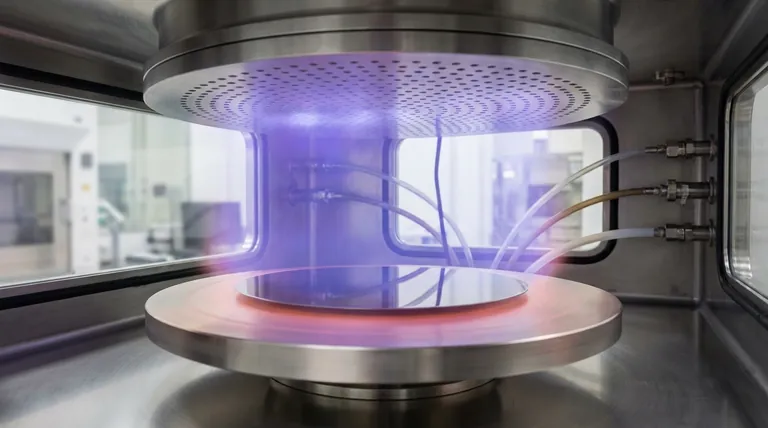
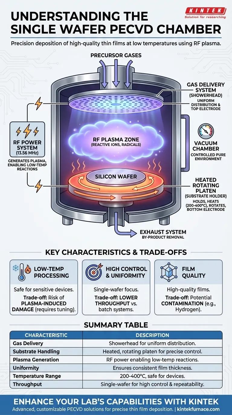
At its core, a single-wafer PECVD chamber is a precisely engineered vacuum environment for depositing high-quality thin films onto a single substrate at low temperatures. Its key characteristics include a "showerhead" for uniform gas delivery, a heated and often rotating platen to hold the wafer, and a radio frequency (RF) power source to generate plasma. This design prioritizes uniformity and control over the deposition process on an individual wafer.
The fundamental design of a single-wafer PECVD chamber revolves around a single principle: using RF-generated plasma to provide the energy for chemical reactions. This allows for high-quality film deposition at temperatures low enough to be safe for sensitive, fully fabricated electronic devices, a task not possible with high-temperature methods like LPCVD.
The Core Components and Their Function
To understand the chamber, you must understand how its components work together to create a controlled plasma environment. Each part serves a specific purpose in achieving a uniform, low-temperature deposition.
The Vacuum Chamber
The chamber itself is typically made of stainless steel with a front-loading door for access. It is pumped down to a vacuum to remove atmospheric gases and contaminants, creating a pure environment for the deposition chemistry. An observation window is often included for process monitoring.
The Gas Delivery System (Showerhead)
Precursor gases are introduced into the chamber through a showerhead. This component is a critical design feature, resembling a literal shower head with many small holes.
Its primary function is to distribute the reactive gases evenly across the entire surface of the wafer, which is essential for achieving uniform film thickness. In many designs, this showerhead also serves as the top electrode for the RF power system.
The Substrate Holder (Platen)
The silicon wafer or other substrate rests on a heated platen, also called a chuck or sample stand. This component has three key functions:
- Holding: It secures the wafer in place.
- Heating: It heats the wafer to a specific, highly controlled process temperature (e.g., 200-400°C), which is significantly lower than in non-plasma methods.
- Rotating: The platen often rotates at a slow, controlled speed (e.g., 1-20 rpm) to further average out any minor non-uniformities in gas flow or plasma density.
In a standard capacitively coupled plasma system, the platen also functions as the bottom, or powered, electrode.
The RF Power System
The radio frequency (RF) power system is what puts the "plasma-enhanced" in PECVD. RF energy, typically at 13.56 MHz, is applied between the showerhead and the platen.
This energy ignites the precursor gases, stripping electrons and creating a plasma—a reactive cloud of ions, radicals, and electrons. This plasma provides the activation energy needed for the chemical reactions to occur on the wafer surface, eliminating the need for very high temperatures.
The Exhaust System
By-product gases from the chemical reaction are removed from the chamber through an exhaust system. The exhaust ports are typically located below the level of the wafer, helping to direct the flow of gas down and away from the substrate surface and maintain the desired chamber pressure.
Understanding the Trade-offs
While single-wafer PECVD is a powerful technique, it is essential to understand its inherent trade-offs. No single method is perfect for all applications.
Plasma-Induced Damage vs. Low Temperature
The primary benefit of PECVD is its low-temperature processing, enabled by the plasma. However, the energetic ions within that same plasma can bombard the wafer surface, potentially causing damage to sensitive electronic device layers. Process engineers must carefully tune RF power and pressure to minimize this damage.
Throughput vs. Control
As the name implies, a single-wafer system processes one substrate at a time. This provides exceptional control and wafer-to-wafer repeatability. The trade-off is lower throughput compared to batch systems (like LPCVD furnaces) that can process dozens or hundreds of wafers at once, albeit with less individual control and at much higher temperatures.
Film Quality and Contamination
Because PECVD reactions occur at lower temperatures and higher pressures than other CVD methods, the resulting films can sometimes incorporate contaminants, such as hydrogen from precursor gases. This can impact the film's electrical or mechanical properties and must be managed through careful recipe development.
Making the Right Choice for Your Application
Your choice of deposition technology should be driven by the specific requirements of your device or material.
- If your primary focus is depositing films on temperature-sensitive devices: PECVD is the superior choice, as the plasma provides reaction energy without requiring heat that could damage existing structures.
- If your primary focus is achieving the highest possible film uniformity: A single-wafer system with a rotating platen and showerhead gas delivery offers the best control for a single, high-value substrate.
- If your primary focus is high-volume production of simple films: A batch processing system may be more cost-effective, provided your substrates can withstand the higher process temperatures.
By understanding these core characteristics and trade-offs, you can confidently determine if a single-wafer PECVD system aligns with your technical and manufacturing goals.
Summary Table:
| Characteristic | Description |
|---|---|
| Gas Delivery | Showerhead for uniform distribution of precursor gases |
| Substrate Handling | Heated, rotating platen for precise wafer control |
| Plasma Generation | RF power system enabling low-temperature reactions |
| Uniformity | Ensures consistent film thickness across the wafer |
| Temperature Range | Operates at 200-400°C, safe for sensitive devices |
| Throughput | Single-wafer processing for high control and repeatability |
Enhance your lab's capabilities with KINTEK's advanced PECVD solutions! Leveraging exceptional R&D and in-house manufacturing, we provide diverse laboratories with high-temperature furnace systems like PECVD, CVD, Muffle, Tube, Rotary, and Vacuum & Atmosphere Furnaces. Our strong deep customization capability ensures we meet your unique experimental needs for precise thin film deposition. Contact us today to discuss how our tailored solutions can optimize your processes and drive innovation!
Visual Guide
Related Products
- Slide PECVD Tube Furnace with Liquid Gasifier PECVD Machine
- RF PECVD System Radio Frequency Plasma Enhanced Chemical Vapor Deposition
- Inclined Rotary Plasma Enhanced Chemical Deposition PECVD Tube Furnace Machine
- Inclined Rotary Plasma Enhanced Chemical Deposition PECVD Tube Furnace Machine
- Split Chamber CVD Tube Furnace with Vacuum Station CVD Machine
People Also Ask
- What is plasma in the context of PECVD? Unlock Low-Temperature Thin Film Deposition
- What are the main advantages of PECVD tube furnaces compared to CVD tube furnaces? Lower Temp, Faster Deposition, and More
- What are the advantages of using a tube furnace CVD system for Cu(111)/graphene? Superior Scalability and Quality
- What are the typical conditions for plasma-enhanced CVD processes? Achieve Low-Temperature Thin Film Deposition
- In which industries is the tube furnace commonly used? Essential for Materials Science, Energy, and More


