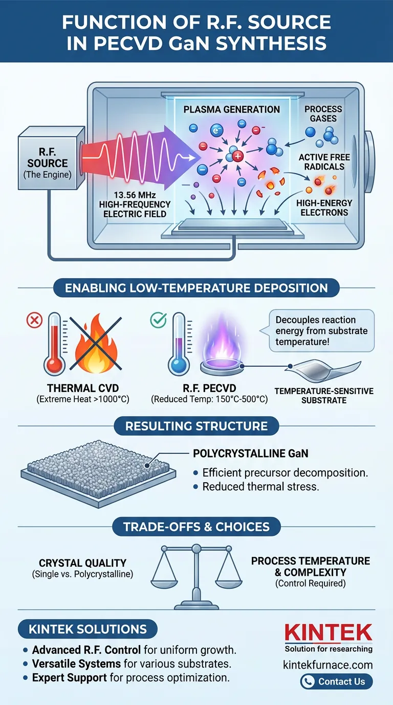
The primary function of the radio frequency (R.F.) source in a Plasma Enhanced Chemical Vapor Deposition (PECVD) system is to generate a high-frequency electric field—typically at 13.56 MHz—that transforms process gases into a reactive plasma state. By providing the energy required to excite and dissociate gas molecules, the R.F. source drives the chemical reactions necessary for Gallium Nitride (GaN) synthesis without relying solely on thermal heat.
By substituting thermal energy with electrical energy to initiate chemical reactions, the R.F. source enables the deposition of GaN films at significantly lower temperatures (e.g., 500 °C), allowing for synthesis on temperature-sensitive substrates while maintaining reaction efficiency.
The Mechanism of Plasma Generation
Creating the Electromagnetic Field
The R.F. source serves as the "engine" of the deposition process. It generates a 13.56 MHz high-frequency electric field within the reaction chamber. This oscillating field is the catalyst that changes the state of the gas environment.
Electron Collision and Ionization
Within this electric field, electrons are accelerated to high energy levels. These high-energy electrons collide with gas molecules, causing them to ionize and dissociate.
Formation of Active Free Radicals
These collisions break down the stable process gases into active free radicals. These radicals are highly reactive chemical species that are primed to bond and form solid structures, effectively preparing the precursors for deposition.
Enabling Low-Temperature Deposition
Overcoming Thermal Limitations
Traditional thermal CVD relies on extreme heat to break chemical bonds, which restricts the types of substrates you can use. The R.F. source creates a high-density plasma that provides the necessary energy for decomposition chemically rather than thermally.
Operating at Reduced Temperatures
Because the plasma drives the reaction, the substrate does not need to be heated to extreme levels. The process facilitates the decomposition of precursors at temperatures as low as 500 °C, and in some configurations, between 150 °C and 500 °C.
Synthesis of Polycrystalline Structures
This specific energy environment is tuned to facilitate the growth of polycrystalline Gallium Nitride (GaN). The R.F. source ensures that the precursors decompose efficiently enough to form these structures without the thermal stress that would damage delicate materials.
Understanding the Trade-offs
Crystal Quality vs. Process Temperature
While the R.F. source enables lower temperatures, this reduction in thermal energy impacts crystal formation. The process typically results in polycrystalline structures rather than single-crystal films often achieved at higher temperatures, which may alter the electrical properties of the final GaN layer.
Complexity of Control
Using an R.F. source introduces variables such as plasma density and ion bombardment energy. These factors must be precisely managed to prevent damage to the growing film or the substrate, adding a layer of complexity compared to purely thermal systems.
Making the Right Choice for Your Goal
When integrating an R.F. source for GaN synthesis, consider your specific application requirements regarding substrate tolerance and film structure.
- If your primary focus is substrate flexibility: Rely on the R.F. source to lower process temperatures (down to 500 °C or lower), enabling deposition on temperature-sensitive materials like polyimide.
- If your primary focus is reaction efficiency: Utilize the R.F. generated plasma to accelerate precursor decomposition rates, bypassing the kinetic limitations of thermal-only activation.
The R.F. source effectively decouples the energy required for chemical reaction from the energy required for substrate heating, offering a critical window for processing advanced GaN materials on diverse platforms.
Summary Table:
| Feature | Function & Impact |
|---|---|
| Primary Frequency | 13.56 MHz High-Frequency Electric Field |
| Key Mechanism | Electron collision and ionization of process gases |
| Energy Source | Electrical energy (plasma) instead of purely thermal heat |
| Operating Temperature | Typically 150°C to 500°C (Enables heat-sensitive substrates) |
| Film Result | Polycrystalline Gallium Nitride (GaN) structures |
| Main Advantage | Decouples reaction energy from substrate temperature |
Optimize Your Thin Film Deposition with KINTEK
Take control of your Gallium Nitride synthesis with precision-engineered PECVD technology. Backed by expert R&D and world-class manufacturing, KINTEK offers a comprehensive range of lab high-temperature furnaces, including CVD, Vacuum, Muffle, and Tube systems, all fully customizable to meet your specific research or production needs.
Why partner with KINTEK?
- Advanced R.F. Control: Achieve stable plasma density for uniform thin-film growth.
- Versatile Solutions: Systems tailored for temperature-sensitive substrates and high-purity polycrystalline GaN.
- Expert Support: Specialized guidance to help you balance crystal quality and process efficiency.
Ready to elevate your material science capabilities? Contact us today to explore our customizable deposition solutions!
Visual Guide
References
- Olzat Toktarbaiuly, Г. Сугурбекова. ENHANCEMENT OF POWER CONVERSION EFFICIENCY OF DYE-SENSITIZED SOLAR CELLS VIA INCORPORATION OF GAN SEMICONDUCTOR MATERIAL SYNTHESIZED IN HOT-WALL CHEMICAL VAPOR DEPOSITION FURNACE. DOI: 10.31489/2024no4/131-139
This article is also based on technical information from Kintek Furnace Knowledge Base .
Related Products
- RF PECVD System Radio Frequency Plasma Enhanced Chemical Vapor Deposition
- Slide PECVD Tube Furnace with Liquid Gasifier PECVD Machine
- Inclined Rotary Plasma Enhanced Chemical Deposition PECVD Tube Furnace Machine
- Inclined Rotary Plasma Enhanced Chemical Deposition PECVD Tube Furnace Machine
- MPCVD Machine System Reactor Bell-jar Resonator for Lab and Diamond Growth
People Also Ask
- How are deposition rates and film properties controlled in PECVD? Master Key Parameters for Optimal Thin Films
- What are the key advantages of PECVD technology? Achieve Low-Temperature, High-Quality Thin Film Deposition
- What are some promising applications of PECVD-prepared 2D materials? Unlock Advanced Sensing and Optoelectronics
- What are the advantages of PECVD in film deposition? Achieve Low-Temp, High-Quality Coatings
- What is PECVD specification? A Guide to Choosing the Right System for Your Lab


