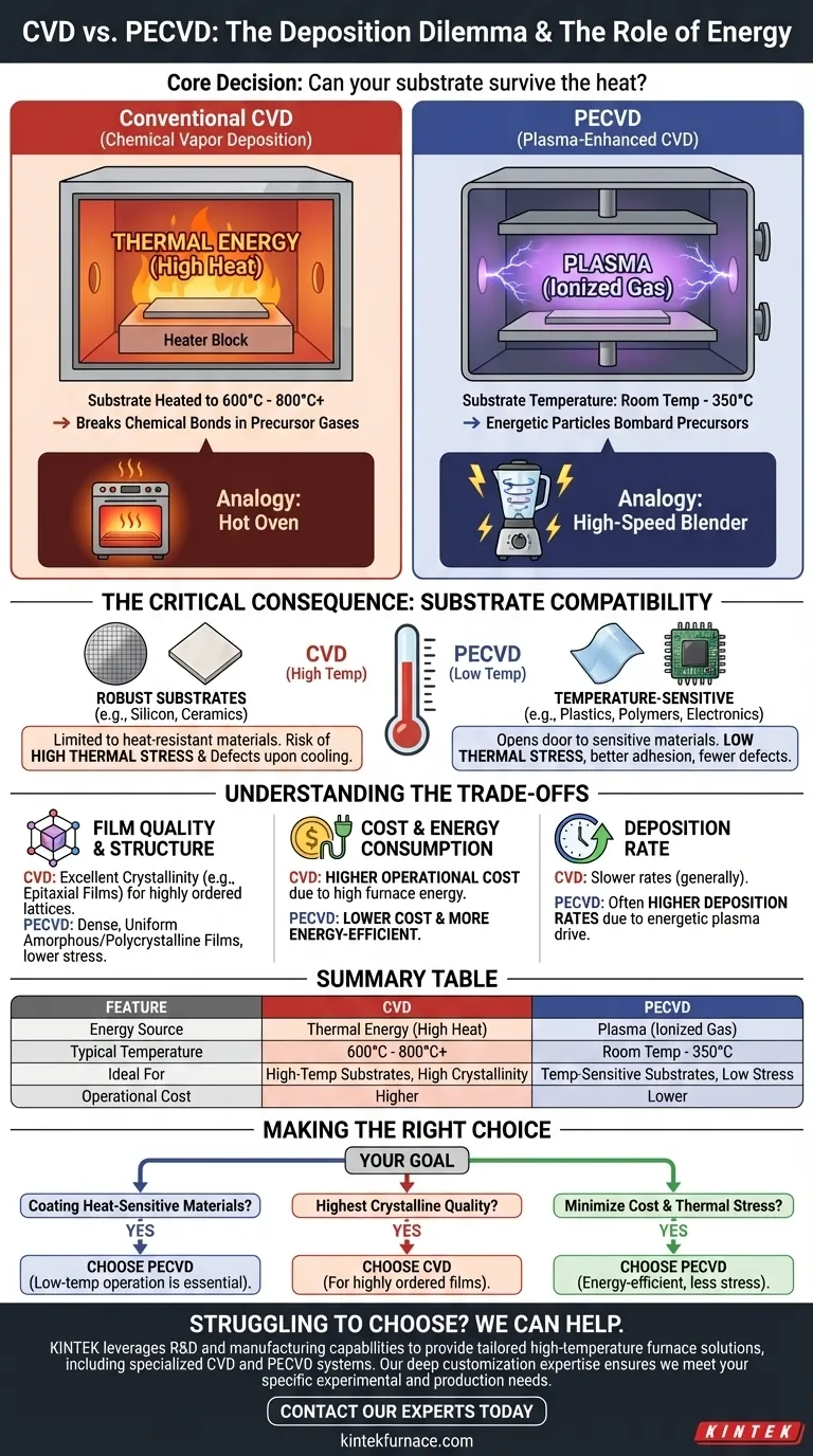
The fundamental difference between Chemical Vapor Deposition (CVD) and Plasma-Enhanced Chemical Vapor Deposition (PECVD) lies in how they supply energy to the deposition process. Conventional CVD uses high heat to trigger chemical reactions, while PECVD uses an energized gas, or plasma, to achieve the same result at much lower temperatures.
The choice between CVD and PECVD is not about which is superior, but which is appropriate. The core decision hinges on one critical factor: whether your substrate material can survive the high temperatures required by conventional CVD.
The Fundamental Difference: How Energy is Supplied
To deposit a thin film, precursor gases must be broken down and made to react. CVD and PECVD take two distinct approaches to providing the energy for this reaction.
How Conventional CVD Works: The Power of Heat
Conventional CVD relies exclusively on thermal energy. The substrate is heated to very high temperatures, typically between 600°C and 800°C, and sometimes even higher.
This intense heat provides the activation energy needed to break the chemical bonds in the precursor gases, allowing them to react and form a solid film on the substrate's surface. Think of it as using a very hot oven to bake a coating onto a surface.
How PECVD Works: The Power of Plasma
PECVD decouples the reaction energy from heat. Instead of a hot oven, it uses what is essentially a high-energy field to create a plasma.
Plasma is an ionized gas containing highly energetic electrons, ions, and free radicals. These particles bombard the precursor gas molecules, breaking them apart and creating reactive species. This allows the deposition reaction to occur without needing high temperatures, with substrate temperatures often ranging from room temperature to 350°C.
This is analogous to using a high-speed blender instead of a stove. The blender's blades (the plasma) break down the ingredients (the precursors) with kinetic energy, not thermal energy.
The Critical Consequence: Deposition Temperature
The difference in energy source leads to a dramatic difference in operating temperature, which has profound implications for the manufacturing process and the final product.
Why Temperature Matters for Substrates
The high temperatures of conventional CVD limit its use to materials that can withstand the heat, such as silicon wafers, ceramics, or certain metals.
PECVD’s low-temperature process opens the door to coating temperature-sensitive substrates like plastics, polymers, and complex electronic components that would be damaged or destroyed by CVD’s thermal budget. This is why PECVD is used for applications like anti-scratch coatings on eyeglass lenses.
Reducing Thermal Stress and Defects
When a film is deposited at a high temperature and then cools, the difference in thermal expansion between the film and the substrate can create significant thermal stress. This stress can lead to cracking, delamination, or other defects.
Because PECVD operates at much lower temperatures, it introduces far less thermal stress, resulting in films with better adhesion, higher density, and fewer pinhole defects.
Understanding the Trade-offs
While PECVD's low temperature is a significant advantage, the choice between the two methods involves considering the desired outcome and operational constraints.
Film Quality and Structure
PECVD is known for producing high-quality amorphous or polycrystalline films that are dense and uniform. The lower stress environment is a major benefit.
However, for applications requiring highly ordered, single-crystal films, the high heat of conventional CVD can be an advantage, as it provides the thermal energy necessary for atoms to arrange themselves into a perfect crystalline lattice.
Cost and Energy Consumption
The high-temperature requirement of CVD furnaces translates directly to high energy consumption and, consequently, higher operational costs.
PECVD systems, operating at or near room temperature, are significantly more energy-efficient. This can lead to substantial cost savings, especially in high-volume manufacturing.
Deposition Rate
By using plasma, PECVD can often achieve higher deposition rates than thermal CVD processes. The energetic plasma environment actively drives the reaction forward, allowing films to be grown more quickly.
Making the Right Choice for Your Goal
Selecting the correct deposition method requires matching the process capabilities to your specific technical and business goals.
- If your primary focus is coating heat-sensitive materials: PECVD is the clear and often only choice due to its low-temperature operation.
- If your primary focus is achieving the highest crystalline quality on a robust substrate: Conventional CVD is often the preferred method for creating highly ordered epitaxial films.
- If your primary focus is minimizing operational costs and thermal stress: PECVD offers a more energy-efficient and less mechanically stressful process for producing high-quality films.
Ultimately, understanding the role of energy in each process empowers you to select the right tool for creating your desired material on your specific substrate.
Summary Table:
| Feature | CVD (Chemical Vapor Deposition) | PECVD (Plasma-Enhanced CVD) |
|---|---|---|
| Energy Source | Thermal Energy (High Heat) | Plasma (Ionized Gas) |
| Typical Temperature | 600°C - 800°C+ | Room Temperature - 350°C |
| Ideal For | High-Temperature Substrates (e.g., Silicon, Ceramics) | Temperature-Sensitive Substrates (e.g., Plastics, Polymers) |
| Film Quality | Excellent Crystallinity (e.g., Epitaxial Films) | Dense, Uniform Amorphous/Polycrystalline Films |
| Operational Cost | Higher (Due to High Energy Consumption) | Lower (More Energy-Efficient) |
Struggling to choose the right deposition process for your unique substrate and performance requirements?
At KINTEK, we leverage our exceptional R&D and in-house manufacturing capabilities to provide advanced high-temperature furnace solutions, including our specialized CVD and PECVD systems. Our deep customization expertise ensures we can precisely tailor the equipment to meet your specific experimental and production needs, whether you require high-crystallinity films on robust substrates or low-temperature coatings on sensitive materials.
Contact our experts today to discuss your project and discover how our tailored solutions can optimize your thin-film deposition process.
Visual Guide
Related Products
- Inclined Rotary Plasma Enhanced Chemical Deposition PECVD Tube Furnace Machine
- Inclined Rotary Plasma Enhanced Chemical Deposition PECVD Tube Furnace Machine
- RF PECVD System Radio Frequency Plasma Enhanced Chemical Vapor Deposition
- Slide PECVD Tube Furnace with Liquid Gasifier PECVD Machine
- Custom Made Versatile CVD Tube Furnace Chemical Vapor Deposition CVD Equipment Machine
People Also Ask
- What is plasma in the context of PECVD? Unlock Low-Temperature Thin Film Deposition
- What plasma source is used in PE-CVD tube furnaces? Unlock Low-Temperature, High-Quality Deposition
- What are the typical conditions for plasma-enhanced CVD processes? Achieve Low-Temperature Thin Film Deposition
- What are some applications of rotary tube furnaces? Ideal for Continuous High-Temperature Material Processing
- How does the temperature control system work in a rotary tube furnace? Achieve Precise Thermal Processing for Your Materials


