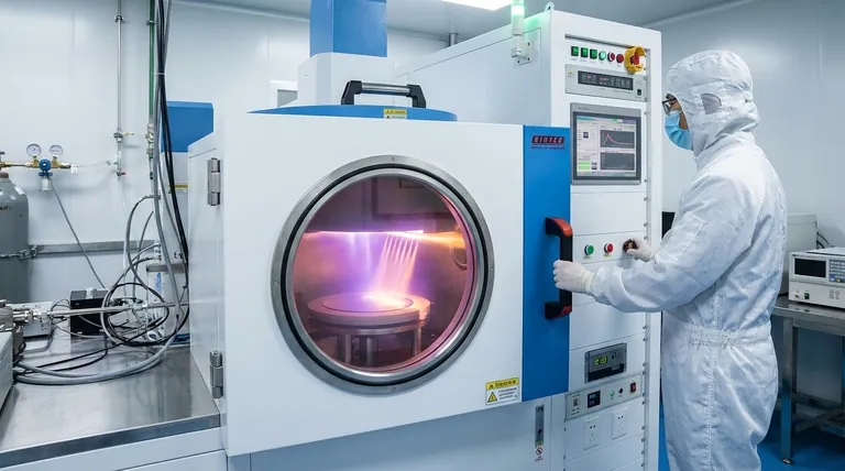
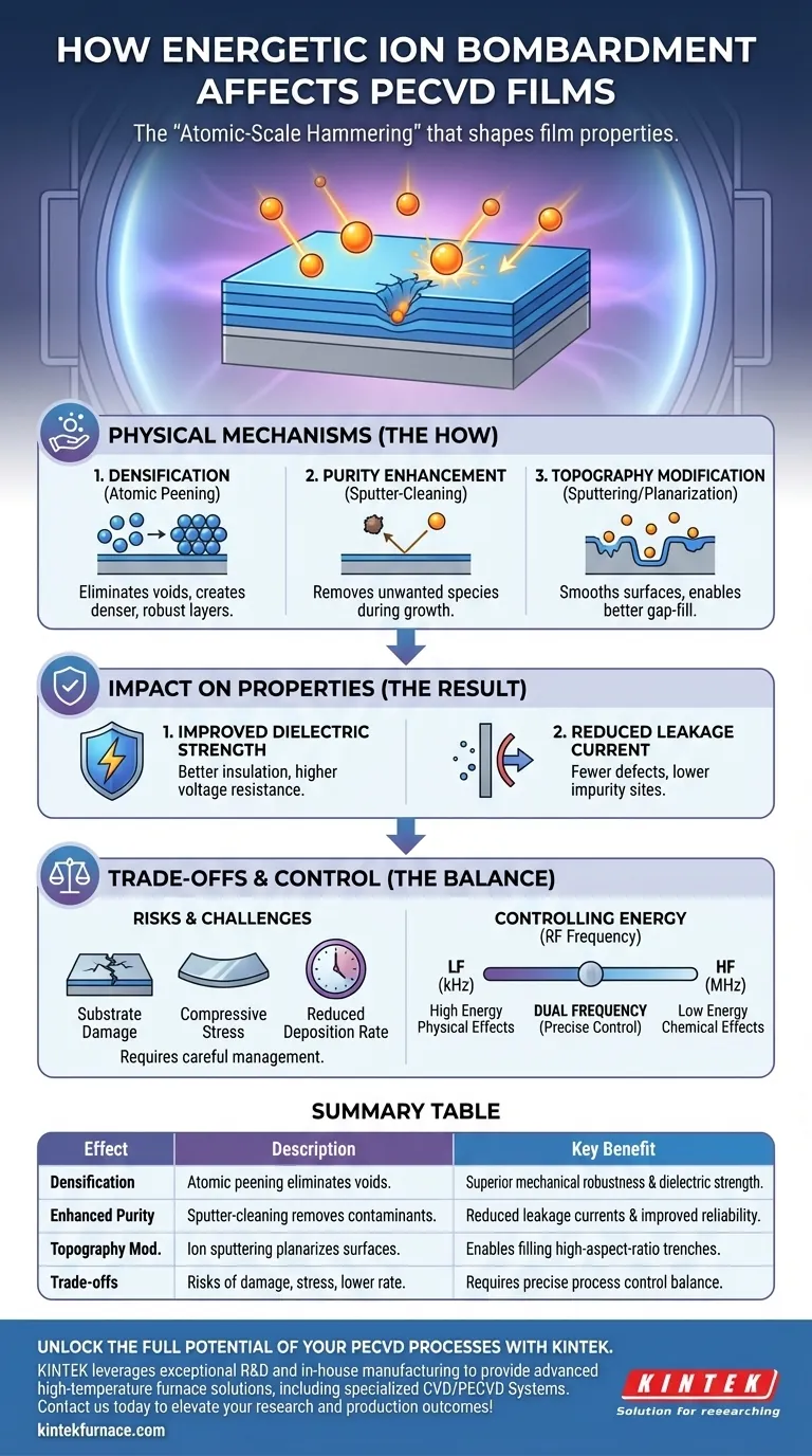
At its core, energetic ion bombardment in Plasma-Enhanced Chemical Vapor Deposition (PECVD) is a physical process that fundamentally alters how a film grows. Instead of atoms simply settling onto a surface, they are simultaneously bombarded by high-energy ions from the plasma. This "atomic-scale hammering" densifies the film, cleanses its surface during growth, and can even be used to reshape the film's topography for specific applications.
Ion bombardment is not merely a side effect of the plasma; it is a critical control lever. By tuning the energy of these ions, engineers can precisely tailor a film's physical density, purity, stress, and electrical performance to meet the demands of a specific device.
The Physical Mechanisms of Ion Bombardment
To understand the impact, we must first look at the physical interactions happening at the substrate surface. The energy transferred by each ion impact drives several key processes simultaneously.
Driving Film Densification
Ions striking the surface transfer kinetic energy to the freshly deposited atoms. This energy allows atoms to move and rearrange themselves into a more tightly packed structure.
This process, known as atomic peening, effectively eliminates voids that would otherwise form in the film. The result is a denser, more physically robust layer with superior mechanical properties.
Enhancing Film Purity
During deposition, unwanted contaminants or weakly bonded precursor fragments can land on the surface. Energetic ions can knock these species off the surface before they are buried by subsequent layers.
This sputter-cleaning effect acts as a continuous purification step during growth. It ensures the final film is composed primarily of the desired material, which is critical for electrical performance.
Modifying Surface Topography
In high-density plasmas, ion bombardment can be intense enough to cause significant sputtering of the deposited film itself. While this may sound counterproductive, it is a powerful tool for planarization.
Ions tend to sputter corners and high points more readily than flat surfaces or the bottom of trenches. This effect helps smooth the surface as it grows, enabling superior gap-fill performance for filling deep trenches or holes in microelectronic structures.
Impact on Electrical and Material Properties
The physical changes induced by ion bombardment have a direct and significant effect on the film's final performance characteristics.
Improving Dielectric Strength
A denser film with fewer voids is a better electrical insulator. The lack of empty spaces or defect pathways means a higher voltage is required to cause a dielectric breakdown.
This results in films with high dielectric strength, a crucial requirement for insulating layers in integrated circuits and passivation layers on semiconductor devices.
Reducing Leakage Current
The same principles apply to leakage current. A pure, dense film has fewer defects and impurity sites that can act as conductive pathways.
By removing contaminants and minimizing voids, ion bombardment directly contributes to films with low leakage currents, ensuring components operate efficiently and reliably.
Understanding the Trade-offs
While powerful, energetic ion bombardment is not a universally beneficial process. Its application requires a careful balance to avoid negative consequences.
The Risk of Substrate Damage
Excessively high ion energies can do more than just densify the film; they can penetrate into the underlying substrate.
This can create crystal lattice defects in the substrate, damaging sensitive electronic devices. This is a primary reason why ion energy must be precisely controlled.
Inducing Compressive Stress
The constant "hammering" from ions compacts the film, often resulting in high levels of compressive stress.
If not managed, this stress can cause the film to delaminate from the substrate or even cause the entire wafer to bow or warp, complicating subsequent processing steps.
Deposition Rate vs. Sputtering
Aggressive ion bombardment sputters away material as it is being deposited. This creates a competition between the deposition rate and the sputtering rate.
In some high-energy regimes, the net deposition rate can be significantly reduced or even become negative (etching). This trade-off between film quality and process throughput must be carefully managed.
Controlling Ion Energy: The Role of Frequency
The key to harnessing ion bombardment is controlling ion energy, which is primarily achieved by manipulating the radio frequency (RF) used to generate the plasma.
Low-Frequency (LF) Systems
Frequencies in the kilohertz (kHz) range allow ions enough time to accelerate across the plasma sheath and strike the substrate with high energy. This approach is ideal when physical effects like densification or sputter-planarization are the primary goal.
High-Frequency (HF) Systems
The industry-standard 13.56 MHz frequency results in a rapidly oscillating sheath potential. Most heavy ions are too massive to respond to these fast changes, so they strike the substrate with much lower energy. This favors chemical reaction pathways over physical bombardment.
Dual-Frequency Systems: The Modern Solution
Modern PECVD reactors often use a dual-frequency approach, mixing a high frequency (like 13.56 MHz) with a low frequency (kHz range). The HF source primarily controls the plasma density (the number of ions), while the LF source independently controls the ion energy. This decoupling provides the ultimate process control.
Tailoring Ion Bombardment to Your Goal
The optimal level of ion bombardment is entirely dependent on the desired film properties and application.
- If your primary focus is a dense, mechanically hard film: Use a process with higher ion energy (e.g., lower frequency bias) to maximize atomic peening.
- If your primary focus is filling high-aspect-ratio trenches: Employ a balanced process where ion-driven sputtering helps planarize the surface as it deposits.
- If your primary focus is depositing on a sensitive substrate or maximizing deposition rate: Use lower ion energy (e.g., a high-frequency-only process) to minimize damage and sputtering.
Ultimately, mastering energetic ion bombardment transforms it from a simple process variable into a precise tool for engineering thin films at the atomic scale.
Summary Table:
| Effect | Description | Key Benefit |
|---|---|---|
| Film Densification | Atomic peening eliminates voids, creating tightly packed structures. | Superior mechanical robustness and higher dielectric strength. |
| Enhanced Purity | Sputter-cleaning removes contaminants during deposition. | Reduced leakage currents and improved electrical reliability. |
| Surface Topography Modification | Ion sputtering planarizes surfaces for better gap-fill. | Enables filling of high-aspect-ratio trenches in microelectronics. |
| Trade-offs | Includes risk of substrate damage, compressive stress, and reduced deposition rate. | Requires precise control to balance film quality and process throughput. |
Unlock the Full Potential of Your PECVD Processes with KINTEK
Are you aiming to achieve superior film density, enhanced purity, and tailored electrical properties in your semiconductor or laboratory applications? KINTEK leverages exceptional R&D and in-house manufacturing to provide advanced high-temperature furnace solutions, including our specialized CVD/PECVD Systems. With strong deep customization capabilities, we precisely meet your unique experimental requirements, ensuring optimal performance in film deposition.
Contact us today to discuss how our expertise can elevate your research and production outcomes!
Visual Guide
Related Products
- Slide PECVD Tube Furnace with Liquid Gasifier PECVD Machine
- RF PECVD System Radio Frequency Plasma Enhanced Chemical Vapor Deposition
- Inclined Rotary Plasma Enhanced Chemical Deposition PECVD Tube Furnace Machine
- Inclined Rotary Plasma Enhanced Chemical Deposition PECVD Tube Furnace Machine
- Multi Heating Zones CVD Tube Furnace Machine for Chemical Vapor Deposition Equipment
People Also Ask
- What role does a Tube Furnace play in the CVD growth of carbon nanotubes? Achieve High-Purity CNT Synthesis
- In which industries is the tube furnace commonly used? Essential for Materials Science, Energy, and More
- What are the main advantages of PECVD tube furnaces compared to CVD tube furnaces? Lower Temp, Faster Deposition, and More
- What are the advantages of using a tube furnace CVD system for Cu(111)/graphene? Superior Scalability and Quality
- What is plasma in the context of PECVD? Unlock Low-Temperature Thin Film Deposition


