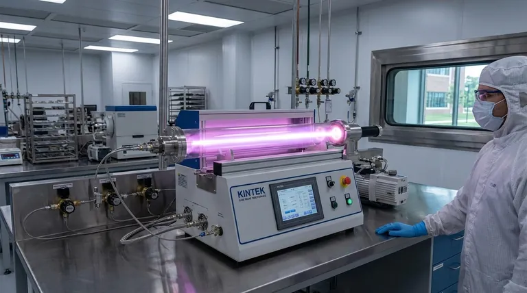
At its core, Plasma-Enhanced Chemical Vapor Deposition (PECVD) is a sophisticated process for depositing very thin, high-performance films of material onto a substrate. Unlike traditional methods that rely on extreme heat, PECVD uses an energized gas, or plasma, to drive the necessary chemical reactions. This allows for high-quality film deposition at significantly lower temperatures, making it an indispensable technique for manufacturing modern electronics like semiconductors and solar cells.
The fundamental advantage of PECVD is its use of plasma energy instead of intense heat. This decoupling of the reaction energy from the substrate temperature allows for the creation of advanced materials on sensitive components that would be damaged or destroyed by traditional high-temperature processes.
How PECVD Differs from Conventional Deposition
To grasp the value of PECVD, it's essential to understand what it improves upon. The traditional method is Chemical Vapor Deposition (CVD), which works on a very different principle.
The Principle of Thermal CVD
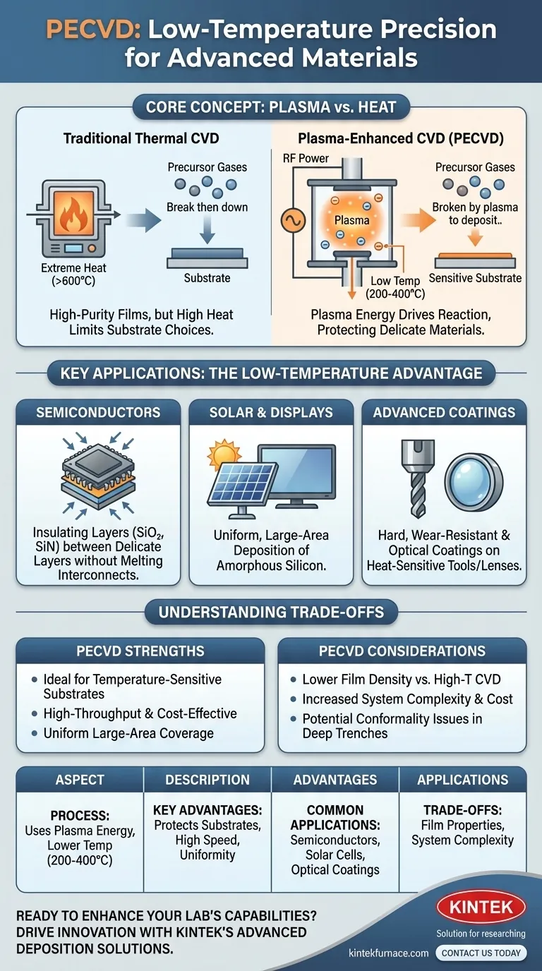
Traditional CVD is analogous to baking a glaze onto pottery. Precursor gases are introduced into a very hot chamber, and the thermal energy from the heated substrate (often >600°C) is what breaks the gas molecules apart and causes them to react and deposit as a solid film.
This method produces excellent, high-purity films but has a major limitation: the substrate itself must be able to withstand extreme temperatures.
The Innovation of Plasma Energy in PECVD
PECVD replaces most of this intense heat with energy from a plasma. By applying an electric field to the precursor gas, we create a plasma—a state of matter containing highly energetic electrons.
These electrons, not the substrate's heat, collide with the gas molecules and break them apart. This allows the chemical deposition reactions to occur on a much cooler substrate, typically in the 200-400°C range.
Key Applications Driven by the Low-Temperature Advantage
The ability to deposit films without high heat unlocks capabilities across numerous high-tech industries. The application isn't just about the film itself, but about what you can safely apply it to.
Semiconductor Fabrication
Modern microchips contain billions of transistors built in complex, stacked layers. PECVD is used to deposit critical insulating films, like silicon dioxide (SiO₂) and silicon nitride (SiN), between these layers.
Using high-temperature CVD would melt the delicate metal interconnects and ruin the underlying device structures. PECVD allows these high-quality insulating layers to be added without damaging the work already done.
Solar Cell and Display Manufacturing
PECVD is critical for depositing films like amorphous silicon over very large areas. Its ability to achieve uniform films at relatively high speeds and moderate temperatures is essential for the cost-effective production of solar panels and flat-panel displays.
Advanced Protective and Optical Coatings
PECVD can apply hard, wear-resistant coatings to materials like cutting tools without altering the temper of the underlying metal. It is also used to deposit precise layers of materials for optical coatings on lenses and sensors, controlling how they reflect or transmit light.
Understanding the Trade-offs
No technology is a universal solution. While powerful, PECVD has considerations that make it more suitable for some tasks than others.
Film Properties vs. Temperature
While PECVD films are high quality, films grown at very high temperatures via traditional CVD can sometimes achieve higher density or structural perfection. The lower-energy PECVD process can sometimes leave trace elements, like hydrogen, from the precursor gas in the final film, which can affect its electrical or mechanical properties.
System and Process Complexity
A PECVD system is inherently more complex than a simple thermal CVD furnace. It requires a vacuum chamber, precise gas flow control, and a radio-frequency (RF) power source to generate and sustain the plasma. This adds layers of cost and process control complexity.
Coating Uniformity (Conformality)
The nature of the plasma-driven process can sometimes make it more difficult to achieve a perfectly uniform coating inside very deep and narrow trenches on a substrate's surface. In these specific cases, a purely thermal process, which is less "directional," may provide better coverage.
Making the Right Choice for Your Goal
Selecting a deposition method requires aligning the process capabilities with your primary objective and material constraints.
- If your primary focus is depositing films on temperature-sensitive substrates: PECVD is the definitive choice due to its signature low-temperature operation.
- If your primary focus is achieving the highest possible film purity on a robust substrate: A high-temperature thermal CVD process may be more suitable, provided the substrate can withstand the heat.
- If your primary focus is high-throughput manufacturing for applications like solar cells or displays: PECVD offers a compelling balance of deposition speed, film quality, and cost-effectiveness over large areas.
Ultimately, understanding the interplay between plasma energy and thermal energy empowers you to select the most effective deposition strategy for your specific engineering challenge.
Summary Table:
| Aspect | Description |
|---|---|
| Process | Uses plasma energy to deposit thin films at lower temperatures (200-400°C) vs. traditional CVD (>600°C). |
| Key Advantages | Enables deposition on temperature-sensitive substrates; ideal for semiconductors, solar cells, and protective coatings. |
| Common Applications | Semiconductor fabrication (e.g., SiO₂, SiN films), solar panel production, optical coatings, and wear-resistant layers. |
| Trade-offs | May have lower film density than high-temperature CVD; involves higher system complexity and cost. |
Ready to enhance your lab's capabilities with advanced deposition solutions? At KINTEK, we leverage exceptional R&D and in-house manufacturing to provide high-temperature furnace solutions tailored for diverse laboratories. Our product line includes Muffle, Tube, Rotary Furnaces, Vacuum & Atmosphere Furnaces, and CVD/PECVD Systems, all supported by strong deep customization to meet your unique experimental needs. Whether you're working on semiconductors, solar cells, or other high-tech applications, our expertise ensures precise, efficient results. Contact us today to discuss how we can optimize your processes and drive innovation in your projects!
Visual Guide
Related Products
- RF PECVD System Radio Frequency Plasma Enhanced Chemical Vapor Deposition
- Slide PECVD Tube Furnace with Liquid Gasifier PECVD Machine
- Inclined Rotary Plasma Enhanced Chemical Deposition PECVD Tube Furnace Machine
- Inclined Rotary Plasma Enhanced Chemical Deposition PECVD Tube Furnace Machine
- MPCVD Machine System Reactor Bell-jar Resonator for Lab and Diamond Growth
People Also Ask
- What are the key advantages of PECVD technology? Achieve Low-Temperature, High-Quality Thin Film Deposition
- What is PECVD specification? A Guide to Choosing the Right System for Your Lab
- How is silicon dioxide deposited from tetraethylorthosilicate (TEOS) in PECVD? Achieve Low-Temperature, High-Quality SiO2 Films
- What are the applications of plasma enhanced chemical vapor deposition? Key Uses in Electronics, Optics & Materials
- What are the advantages of PECVD in film deposition? Achieve Low-Temp, High-Quality Coatings


